SLWS245B May 2014 – February 2017 TRF3722
PRODUCTION DATA.
- 1 Features
- 2 Applications
- 3 Description
- 4 Revision History
- 5 Pin Configuration and Functions
-
6 Specifications
- 6.1 Absolute Maximum Ratings
- 6.2 ESD Ratings
- 6.3 Recommended Operating Conditions
- 6.4 Thermal Information
- 6.5 Electrical Characteristics
- 6.6 Typical Characteristics
- 6.7 Typical Characteristics - Output Power
- 6.8 Typical Characteristics - Gain
- 6.9 Typical Characteristics - OIP3
- 6.10 Typical Characteristics - OIP2
- 6.11 Typical Characteristics - OP1dB
- 6.12 Typical Characteristics - Noise
- 6.13 Typical Characteristics - Unadjusted CF
- 6.14 Typical Characteristics - Unadjusted SBS
- 6.15 Typical Characteristics - LO Harmonic
- 6.16 Typical Characteristics - BB Harmonic
- 6.17 Typical Characteristics - RF Output Return Loss
- 6.18 Typical Characteristics - PLL/VCO
- 6.19 Typical Characteristics - Current Consumption
- 6.20 Typical Characteristics - Power Dissipation
- 7 Parameter Measurement Information
- 8 Detailed Description
- 9 Application and Implementation
- 10Power Supply Recommendations
- 11Layout
- 12Device and Documentation Support
- 13Mechanical, Packaging, and Orderable Information
Package Options
Mechanical Data (Package|Pins)
- RGZ|48
Thermal pad, mechanical data (Package|Pins)
- RGZ|48
Orderable Information
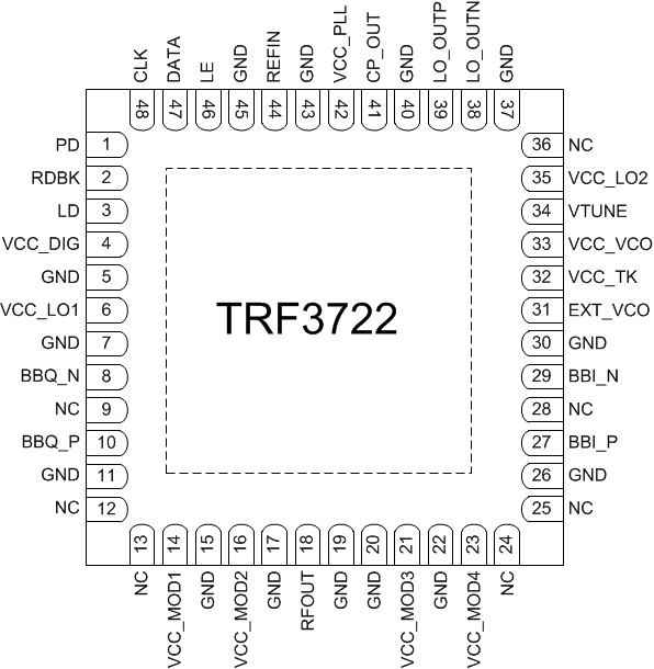
5 Pin Configuration and Functions
RGZ Package
48-Pin VQFN
Top View

Pin Functions
| PIN | I/O | DESCRIPTION | |
|---|---|---|---|
| NAME | NO. | ||
| BBI_N | 29 | I | BB in-phase input: negative |
| BBI_P | 27 | I | BB in-phase input: positive |
| BBQ_N | 8 | I | BB quadrature input: negative |
| BBQ_P | 10 | I | BB quadrature input: positive |
| CLK | 48 | I | Serial interface clock input; digital input |
| CP_OUT | 41 | O | Charge pump output |
| DATA | 47 | I | Serial interface data input; digital input |
| EXT_VCO | 31 | I | External local oscillator input |
| GND | 5, 7, 11, 15, 17, 19, 20, 22, 26, 30, 37, 40, 43, 45 | Ground | |
| LD | 3 | O | PLL lock detect output |
| LE | 46 | I | Serial interface latch enable; digital input |
| LO_OUTN | 38 | O | Local oscillator output: negative |
| LO_OUTP | 39 | O | Local oscillator output: positive |
| NC | 9, 12, 13, 24, 25, 36 | No connect | |
| NC | 28 | No connect; N/C or ground to paddle | |
| PD | 1 | I | LO Div, TX Div, modulator power down (High = PD) |
| RDBK | 2 | O | Serial interface internal registers readback output |
| REFIN | 44 | I | Reference clock input |
| RFOUT | 18 | O | RF output |
| VCC_DIG | 4 | 3.3 V digital power supply | |
| VCC_LO1 | 6 | 3.3 V TX Div power supply | |
| VCC_LO2 | 35 | 3.3 V LO Div power supply | |
| VCC_MOD1 | 14 | 3.3 V modulator power supply | |
| VCC_MOD2 | 16 | 3.3 V modulator power supply | |
| VCC_MOD3 | 21 | 3.3 V modulator power supply | |
| VCC_MOD4 | 23 | 3.3 V modulator power supply | |
| VCC_PLL | 42 | 3.3 V PLL power supply | |
| VCC_TK | 32 | 3.3 V or 5 V VCO tank power supply | |
| VCC_VCO | 33 | 3.3 V VCO power supply | |
| VTUNE | 34 | I | VCO control voltage input |