SCDS358B November 2014 – February 2015 TS3A227E
PRODUCTION DATA.
- 1 Features
- 2 Applications
- 3 Description
- 4 Simplified Schematic
- 5 Revision History
- 6 Pin Configuration and Functions
- 7 Specifications
- 8 Parameter Measurement Information
-
9 Detailed Description
- 9.1 Overview
- 9.2 Functional Block Diagram
- 9.3 Feature Description
- 9.4 Device Functional Modes
- 9.5 Register Maps
- 9.6
Register Field Descriptions
- 9.6.1 Device ID Register Field Descriptions (Address 00h)
- 9.6.2 Interrupt Register Field Descriptions (Address 01h)
- 9.6.3 Key Press Interrupt Register Field Descriptions (Address 02h)
- 9.6.4 Interrupt Disable Register Field Descriptions (Address 03h)
- 9.6.5 Device Settings Field Descriptions (Address 04h)
- 9.6.6 Key Press Settings 1 Field Descriptions (Address 05h)
- 9.6.7 Key Press Settings 2 Field Descriptions (Address 06h)
- 9.6.8 Switch Control 1 Field Descriptions (Address 07h)
- 9.6.9 Switch Control 2 Field Descriptions (Address 08h)
- 9.6.10 Switch Status 1 Field Descriptions (Address 09h)
- 9.6.11 Switch Status 2 Field Descriptions (Address 0Ah)
- 9.6.12 Detection Results Field Descriptions (Address 0Bh)
- 9.6.13 ADC Output Field Descriptions (Address 0Ch)
- 9.6.14 Threshold 1 Field Descriptions (Address 0Dh)
- 9.6.15 Threshold 2 Field Descriptions (Address 0Eh)
- 9.6.16 Threshold 3 Field Descriptions (Address 0Fh)
- 10Application and Implementation
- 11Power Supply Recommendations
- 12Layout
- 13Device and Documentation Support
- 14Mechanical, Packaging, and Orderable Information
Package Options
Mechanical Data (Package|Pins)
Thermal pad, mechanical data (Package|Pins)
Orderable Information
10 Application and Implementation
10.1 Application Information
Figure 19 shows how a standard application schematic for the TS3A227E. The DSBGA package pin connections will be the same except for the lack of thermal pad. The following sections discuss how the TS3A227E works with different headsets and how the key press detection operates.
10.2 Typical Application
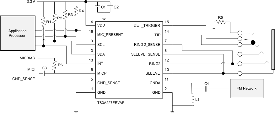 Figure 19. Typical Application Schematic
Table 17. Component List
| COMPONENT | VALUE | NOTES |
|---|---|---|
| R1 | 4.7 kΩ | Pullup resistor must be sized to not exceed max IOL specification for INT pin |
| R2 | 4.7 kΩ | Pullup resistor must be sized to not exceed max IOL specification for INT pin |
| R3 | 4.7 kΩ | Pullup resistor must be sized to not exceed max IOL specification for INT pin |
| R4 | 4.7 kΩ | Pullup resistor must be sized to not exceed max IOL specification for INT pin |
| R5 | 10 kΩ | Pulldown resistor for high to low transition on DET_TRIGGER |
| R6 | 2.2 kΩ ±1% | MICBIAS pullup resistor must be ±1% for Key Press Detection to function properly |
| C1 | 10 µF | De-coupling capacitor for VDD |
| C2 | 100 nF | De-coupling capacitor for VDD |
| C3 | 1 µF | Value can vary depending on codec needs |
| C4 | 47 nF | Value can vary depending on FM matching network needs. If FM transmission is not being supported by the application this capacitor is not needed |
| L1 | 180 nF | Value can vary depending on FM matching network needs. If FM transmission is not being supported by the application this inductor is not needed and GNDA must be shorted to GND |
10.2.1 Design Requirements
10.2.1.1 Standard I2C Interface Details
The bi-directional I2C bus consists of the serial clock (SCL) and serial data (SDA) lines. Both lines must be connected to a positive supply via a pull-up resistor when connected to the output stages of a device. Data transfer may be initiated only when the bus is not busy.
I2C communication with this device is initiated by the master sending a START condition, a high-to-low transition on the SDA line while the SCL line is high. After the start condition, the device address byte is send, MSB first, including the data direction bit (R/W). This device does not respond to the general call address. After receiving the valid address byte (0x77 read, 0x76 write), this device responds with an ACK, a low on the SDA line during the high of the ACK-related clock pulse.
The data byte follows the address ACK. The R/W bit is kept low for transfer from the master to the slave. The data byte is followed by an ACK sent from this device. Data are output only if complete bytes are received and acknowledged. The output data is valid at time (tpv) after the low-to-high transition of SCL, during the clock cycle for the ACK.
On the I2C bus, only one data bit is transferred during each clock pulse. The data on the SDA line must remain stable during the high pulse of the clock period, as changes in the data line at this time are interpreted as control commands (START or STOP).
A Stop condition, a low-to-high transition on the SDA line while the SCL line is high, is sent by the master. The number of data bytes transferred between the start and the stop conditions from the transmitter to receiver is not limited. Each byte of eight bits is followed by one ACK bit. The transmitter must release the SDA line before the receiver can send an ACK bit.
A slave receiver that is addressed must generate an ACK after the reception of each byte. The device that acknowledges has to pull down the SDA line during the ACK clock pulse so that the SDA line is stable low during the high pulse of the ACK-related clock period. Setup and fold times must be taken into account.
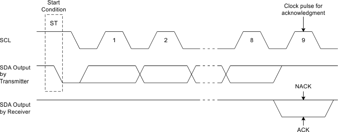 Figure 20. Acknowledgment on the I2C Bus
10.2.1.2 Write Operations
Data is transmitted to the TS3A227E by send the device salve address and setting the LSB to a logic 0. The command byte is sent after the address and determines which register receives the data that follows the command byte. The next byte is written to the specified register on the rising edge of the ACK clock pulse. See Figure 2 and Figure 3 for different modes of write operations.
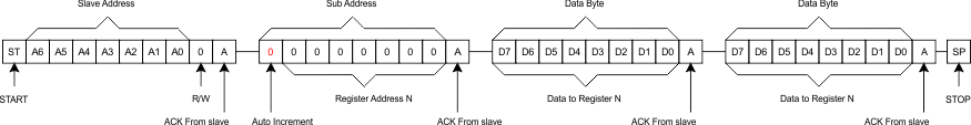 Figure 21. Repeated Data Write to a Single Register
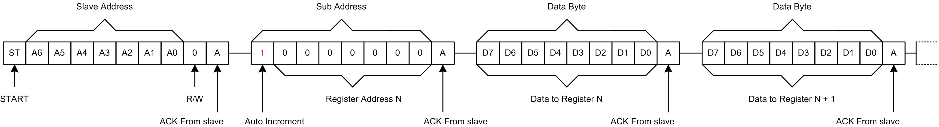 Figure 22. Burst Data Write to Multiple Registers
10.2.1.3 Read Operations
The bus master must send the TS3A227E slave address with the LSB set to logic 0. The command byte is sent after the address and determines which register is accessed. After a restart, the device slave address is sent again but this time the LSB is set to logic 1. Data from the register defined by the command byte then is sent back to the host by the TS3A227E. Data is clicked into the SDA output shift register on the rising edge of the ACK clock pulse. Figure 23 and Figure 24 show read operations that use a restart between the sub-address write and the read operation. A Stop and start condition between the sub-address write and the read operation is also acceptable.
| Notes: | ||
| 1. | SDA is pulled low on ACK from the slave or master. | |
| 2. | Register write always a require sub-address write before writing the first data. | |
| 3. | Repeated data writes to a single register continue indefinitely until n I2C Stop or Re-start. | |
| 4. | Repeated data reads from a single register continue indefinitely until an I2C NACK is received from the master | |
| 5. | Burst data writes start at the specified register address, then advance to the next register address, even to the read-only registers and continue until the Stop or Re-start. For the read-only registers, data write appears to occur, although the register contents are not changed by the write operations. | |
| 6. | Burst data reads start at the specified register address, then advance to the next register address and continues until an I2C NACK is received from the master. | |
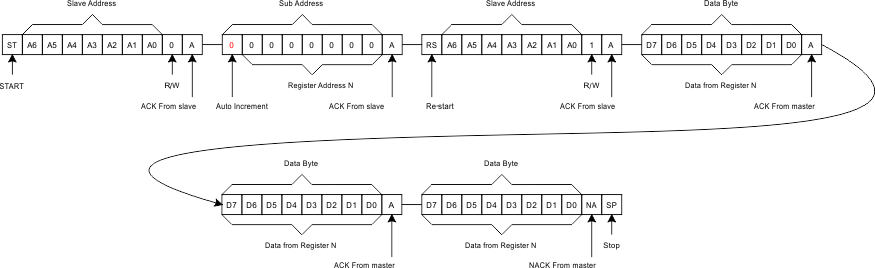 Figure 23. Repeated Data Read From a Single Register
Figure 24. Burst Data Read From Multiple Registers
Figure 23. Repeated Data Read From a Single Register
Figure 24. Burst Data Read From Multiple Registers
10.2.2 Detailed Design Procedure
10.2.2.1 Accessory Insertion
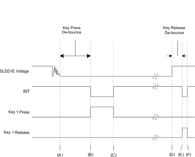
The TS3A227E monitors the DET_TRIGGER pin to determine when an insertion event occurs. A high to low transition one the DET_TRIGGER pin will start the internal de-bounce timer (default 90 ms). This transition is shown in Figure 19. Once the de-bounce timer has expired, it is determined that an accessory is inserted and the detection algorithm is performed to determine what the accessory is and where the ground line is located.
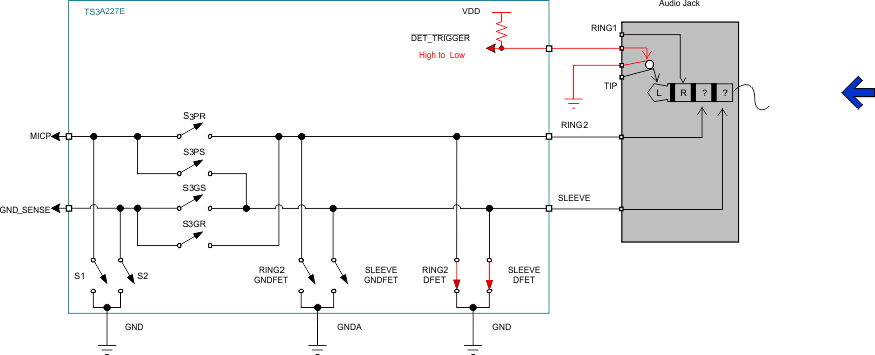 Figure 25. DET_TRIGGER Transition Diagram
Once a DET_TRIGGER transition has occurred, any I2C register changes will not be serviced until after the de-bounce and detection sequence have completed. If DET_TRIGGER transitions from Low to High before the de-bounce period has expired. The I2C register changes will be serviced before a new de-bounce timer is started from another High to Low transition on the DET_TRIGGER pin. The I2C communication has to complete before the next High to Low transition to take effect.
10.2.2.2 Audio Jack Selection
The audio jack the system uses plays a key role in how the system performs and the experience the end user has with the equipment. In real-world scenarios a user might plug in the headset to the audio jack very slowly. This creates a challenging case for the TS3A227E detection mechanism and detection error can occur if care is not taken when designing the components around the TS3A227E.
The main concern for slow plug-in is the detection process may have already started before the headset is fully inserted into the jack. If the detection is running with the headset out of position, a false impedance measurement may occur. For best performance a jack should be chosen that puts the detection mechanism on the TIP pin at the end of physical jack to ensure that it is fully inserted.
The TS3A227E EVM contains test points for all the jack pins and can be blue wired to prototype audio jacks for testing.
10.2.2.3 Switch Status
Table 18 depicts the switch status for each device configuration. A switch diagram is provided in Figure 26.
Table 18. Switch Status
| Device State | S1 | S2 | S3PS | S3PR | S3GS | S3GR | RING2 GNDFET |
SLEEVE GNDFET |
RING2 DFET |
SLEEVE DFET |
|---|---|---|---|---|---|---|---|---|---|---|
| Default State (No insertion or VDD = 0 V) | High-Z | High-Z | High-Z | High-Z | High-Z | High-Z | High-Z | High-Z | On | On |
| Detection running | High-Z | On | High-Z | High-Z | High-Z | High-Z | High-Z | High-Z | High-Z | High-Z |
| 3-pole | On | High-Z | High-Z | High-Z | On | On | On | On | On | On |
| 3-pole with FM support | On | High-Z | High-Z | High-Z | High-Z | On | On | High-Z | High-Z | High-Z |
| 4-pole OMTP | High-Z | High-Z | High-Z | On | On | High-Z | High-Z | On | High-Z | On |
| 4-pole OMTP with FM support | High-Z | High-Z | High-Z | On | On | High-Z | High-Z | On | High-Z | High-Z |
| 4-pole Standard | High-Z | High-Z | On | High-Z | High-Z | On | On | High-Z | On | High-Z |
| 4-pole Standard with FM support | High-Z | High-Z | On | High-Z | High-Z | On | On | High-Z | High-Z | High-Z |
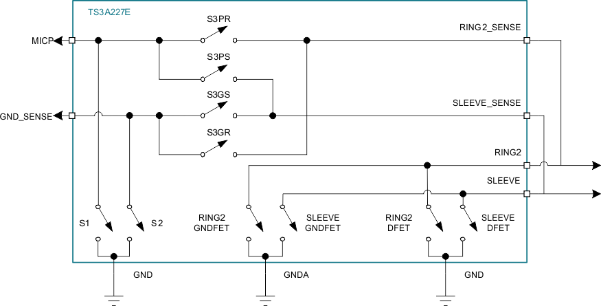 Figure 26. Switch Diagram
10.2.2.3.1 Switch Status Diagrams
Closed switches are red in Figure 27 through Figure 31. The diagrams reflect switch states when manual switch control is not enabled.
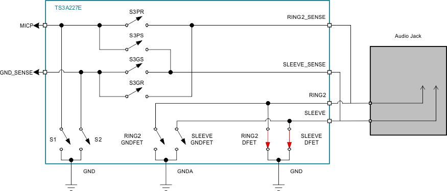 Figure 27. Default Switch State With No Accessory Inserted
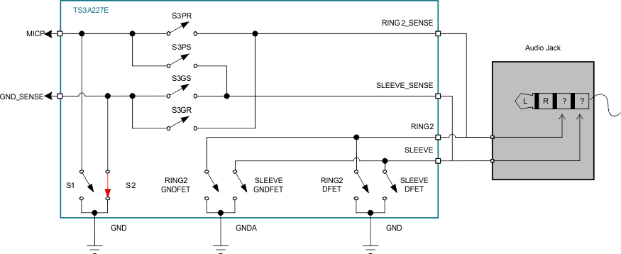 Figure 28. Switch State During Detection
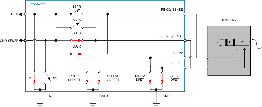 Figure 29. Switch State After Detecting a 3-Pole Headphone
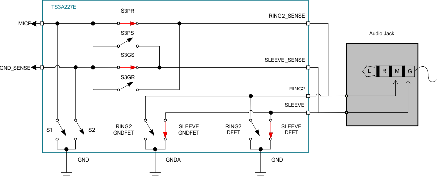 Figure 30. Switch State After Detection a 4-pole OMTP Headset
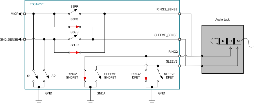 Figure 31. Switch State After Detecting a 4-Pole Standard Headset
10.2.2.4 Key Press Detection
10.2.2.4.1 Key Press Thresholds
The TS3A227E features the ability to adjust the key press thresholds on the fly. The default key press bins are shown below with the default values of the threshold registers optimized to detect these keys. The values for the bins represent the equivalent resistance of the key being pressed with the microphone in parallel. Any equivalent resistance outside these bins is not guaranteed to be detected correctly.
| KEY | TYPICAL RESISTANCE | EQUIVALENT RESISTANCE RANGE |
|---|---|---|
| Key 1 | 50 Ω | 0 Ω – 66 Ω |
| Key 2 | 135 Ω | 126 Ω – 156 Ω |
| Key 3 | 240 Ω | 228 Ω – 264 Ω |
| Key 4 | 470 Ω | 360 Ω – 680 Ω |
The Threshold 1 register (Address 0Dh) adjusts the detection boundary between Key 1 and Key2. The Threshold 2 register (Address 0Eh) adjusts the detection boundary between Key 2 and Key 3. The Threshold 3 register (Address 0Fh adjusts the detection boundary between Key 3 and Key4.
The thresholds are 7 bit values that can be adjusted for the following formula.
It is important for the proper operation of the KP detection algorithm that the thresholds be ordered correctly: KP Threshold 1< KP Threshold 2 < KP Threshold 3. Placing them out of order will cause incorrect keys to be detected. For information on defining the key press gray zones see the Key Press Gray Zones section.
10.2.2.4.2 System Requirements
The Key Press detection algorithm has the following system requirements to be function properly:
- MICBIAS output voltage equivalent to key press settings 2 register value within 2.5%
- MICBIAS pullup resistance equal to 2.2 kΩ ±1%
- Audio jack contact resistance must be limited to < 100 mΩ. See further information below.
Figure 32 depicts the resistor network without the TS3A227E switches for simplicity.
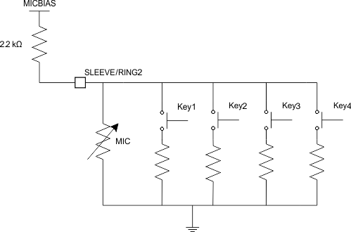 Figure 32. Headset Microphone and Key Network
When the user presses a key it creates a voltage divider network between the MICBIAS output of the codec and the system ground. This will be a measurable voltage on the SLEEVE/RING2 pin that follows Equation 2. Note that this is simplified because it does not include the TS3A227E switches or the contact resistance of the jack itself.
The REQ can be calculated with the following:
As a result of the above calculations, an ADC attempting to detect the voltage on SLEEVE/RING2 to determine which key is pressed (whichever is the microphone pin) is reliant on the accuracy on the MICBIAS output and the 2.2 kΩ pull-up resistor. The key press bins are targeted assuming ideal values for these system conditions and then the gray zone between the bins takes into account the system variations. As a result the better the accuracy of the MICBIAS output and pull-up resistor the better the accuracy of the key press detection.
In addition to the above, the contact resistance of the audio jack itself can play a role in how accurate the key press detection is. A general rule is less contact resistance is better. In the figure below a more complete picture of the system and the voltage the TS3A227E will detect is shown.
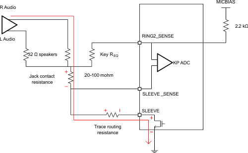
The red line denotes the current path for the output of the codec to follow when it enters the speakers and eventually sinks into the GNDFETs of the TS3A227E. This audio current adds a voltage offset at the audio jack contact resistance, the trace routing resistance, and the GNDFET itself. Because the TS3A227E has kelvin connections to the jack via the SLEEVE_SENSE RING2_SENSE pins the trace routing resistance and GNDFET induced voltage offsets can be compensated.
However, the jack contact resistance is not visible by the device and cannot be compensated for. To maintain the default bin targets the system must ensure that for a given audio jack contact resistance the max current being output by the codec/amplifier lies below the curve in Figure 34. This ensures a max error introduced of 5 mV into the KP detection algorithm.
10.2.2.4.3 Key Press Grey Zones
When defining custom bins and thresholds it is important to also correctly define the “gray zone” between the bins to ensure that the system will always correctly identify the key that is being pressed. The gray zone region accounts for the absolute error in key press detection, encompasses the error of the internal ADC along with errors from system tolerances and variation. The equation below can be used to determine the gray zone required between each of the bins. Note that the size of the gray zone will vary depending on the actual value of the key press threshold.
| TERM | DESCRIPTION | VALUE | UNIT |
|---|---|---|---|
| Ɛ(ADC,GAIN) | Internal ADC gain error | 0.015% | |
| ƐMICBIAS | Codec MICBIAS output voltage variation. Default bin values assume an output variation of 2.5%. | 0.025%(1) | |
| ƐRBIAS | MICBIAS resistor variation. Default bin values assume a 1% tolerance of the 2.2 kΩ MICBIAS resistor. | 0.01%(1) | |
| ƐCONT.GAIN | Gain error introduced by contact resistance of the audio jack. | 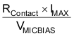 |
|
| ƐKP Threshold | KP threshold target identified by system. E.g. the KP Threshold between bins 1 and 2 for the default key press bins is 96 Ω. | Defined by system(1) | Ω |
| ƐADC,OFF | Internal ADC offset and linearity error | 1.5 | LSB |
| ƐCONT,OFF | Offset error introduced by contact resistance of the audio jack. | 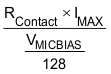 |
LSB |
| KBUFF | Buffer constant added to total system gray zone to ensure bin values are detected correctly. It is recommended to use a minimum of 2 for this when defining key gray zones to ensure system level margins. | 2 | LSB |
| RContact | Max contact resistance of audio jack | Defined by system(1) | Ω |
| IMAX | Maximum combined (Right and Left) audio output current into the jack. | Defined by system(1) | A |
| VMICBIAS | MICBIAS output voltage of the codec | Defined by system(1) | V |
Example Calculation
The default KP Threshold 1 value for the TS3A227E is 10h or 96 Ω. Using the Gray Zone equation the specified gray zone between keys 1 and 2 can be confirmed assuming the following:
- VMICBIAS = 2.2 V
- IMAX × RContact = 5 mV
- R(KP Threshold) = 96 Ω
- Default values for all other terms
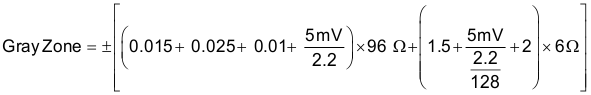
This yields a gray zone of ± 27 Ω. The KP Threshold 1 gray zone can be used to identify the upper limit of key 1 and the lower limit of key 2:
Bin 1 upper limit = KP Threshold 1 – Gray Zone 1
Bin 2 lower limit = KP Threshold 1 + Gray Zone 1
This formula yields an upper limit of 69 Ω. Because each LSB is 6 Ω we round down to the even number of 66 Ω. For the beginning of key 2 we set the value at (96 Ω + 27 Ω) or 126 Ω (123 Ω rounded up to the nearest LSB). This method can be used to define the rest of the key bin thresholds.
10.2.2.4.4 Behavior
The TS3A227E can monitor the microphone line of a 4-pole headset to detect up to 4 key presses/releases and report the key press events back to the host. The key press detection must be activated manually by setting the KP Enable bit of the Device Settings 2 register. To ensure proper operation the MICBIAS voltage must be applied to MICP before enabling key press detection.
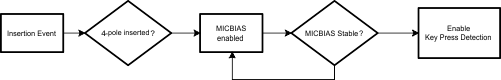 Figure 33. Proper Key Press Enable Sequence
The TS3A227E monitors the S3 switch matrix to determine the location of the microphone. If the Manual Switch Control bit is set to ‘1’, the S3 matrix must be configured in one of the following 2 configurations for the key press detection to operate. Other configurations are not supported with key press detection.
| S3PR | S3PS | S3GR | S3GS | MIC LOCATION |
|---|---|---|---|---|
| On | High-Z | High-Z | On | RING2 |
| High-Z | On | On | High-Z | SLEEVE |
If the voltage on the microphone line drops below the key press detection threshold for a duration longer than the key press de-bounce time, the key press is considered to be valid. At this point the detected key has the corresponding Key # Press interrupt bit set to ‘1’ and the interrupt is asserted. The corresponding Key # Release interrupt is cleared at the same time the Key # Press interrupt is set.
Once the key is released for a duration longer than the key release de-bounce time, a Key Release interrupt is generated to inform the host that the key has been released. The corresponding Key # released interrupt bit is set to ‘1’ and the interrupt is asserted.
The Key Press interrupt register will clear the contents and return to the default status of 0h when Key Press detection is disabled via an I2C write or a removal event.
Notes about key press detection:
- The MICBIAS setting adjusts the detection threshold and must be set to the value that is closest to the MICBIAS output of the codec. If the MICBIAS voltage being used is between different MICBIAS settings of the TS3A227E then the closest value that is greater than the MICBIAS voltage should be used.
- E.G. if the codec output is 2.2 V, the 2.3 V MICBIAS setting in the TS3A227E should be used.
- If any pending interrupt is not read by the host and a key is pressed, the TS3A227E will continue to run key press detection until the Key Press Enable bit is set to ‘0’
The host will interpret Key Press and Release interrupts using the following pseudo-code:
     If (Key # Press && Key # Release) {
            Key # was pressed one time and is not being held.
     }
    else if (Key # Release ) {
            Key # is being pressed, start the key press duration timer
     }
     else if (Key # Release) {
            Key # has been released, end the key press duration timer
     }
The key press duration timer the host starts after reading that a key is pressed can be used as follows:
     If (Key # Press Duration Timer > XXX ms) {
            The Key # is being held down, handle accordingly.

            E.g. if Key # is the volume up key, the system will increment the volume until the Key #
            Release interrupt is read from the TS3A227E
     }
10.2.2.4.5 Single Key Press Timing
The diagram below depicts a key press event where the MIC is on the SLEEVE pin. If the MIC is on RING2 the timing diagram will be same.
10.2.2.4.6 Multiple Key Press Timing
The diagram below depicts a multiple key press event in which the host does not immediately read the interrupt register. The MIC is on the SLEEVE pin in this diagram. If the MIC is on RING2 the timing diagram will be the same.
NOTE
If the KP Enable bit is set to ‘0’ during key press detection, key press detection will stop immediately and all the key press/release bits will be cleared.
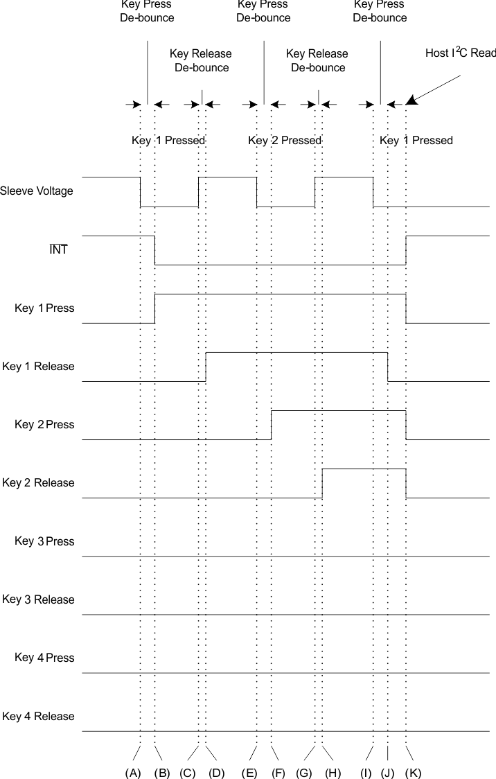
● Key 1 Press
● Key 2 Press
● Key 2 Release
Using the pseudo-code in the key press detection section this is interpreted as:
● Key 2 was pressed one time and is not being held
● Key 1 is currently pressed, start the key press duration timer
10.2.2.4.7 Raw Data Key Press Detection
In addition to threshold adjustment the TS3A227E features the ability to utilize the internal ADC raw output with the Raw Data En bit of the Device Setting 2 register.
Notes on using the Raw ADC Output:
- Key Press/Release interrupts that have not been serviced will not be cleared upon setting the Raw Data En bit to ‘1’.
- By Setting the Raw Data En bit to ‘1’ the Key Press Threshold registers will be ignored. Instead of reporting key 1 through 4 press and releases the TS3A227E will only use Key 1 Press to indicate that a key is pressed and the Key 1 Release interrupt to report that the key was released.
- The ADC Output register will only be cleared after the Raw Data En bit is cleared. The Raw Data En bit is cleared if the Key Press Enable bit is set to ‘0’. Consequently the ADC Output register clears if the Raw Data En bit is set to ‘0’, the Key Press Enable bit is set to ‘0’, or a removal event occurs. This means the ADC Output register will not clear after it is read.
- A manual software trigger can be initiated after a key was pressed to run the ADC detection again. This will not set the Key 1 Press interrupt.
- The ADC Output is updated after a Key is detected or if the manual ADC trigger bit is set to ‘1’. If an ADC conversion has completed the ADC Conversion interrupt bit will be set to ‘1’ regardless if there was a software initiated trigger or if a new key press was detected.
- If the ADC has completed a conversion the output is always non 0 meaning the lowest possible detection threshold of the ADC is 01h. If the ADC Output register is 00h a conversion has not been completed or the ADC Output was cleared.
The previous section on gray zones should be applied to any bins create for the raw ADC mode.
10.2.3 Application Curves
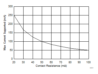 Figure 34. Max Current vs Contact Resistance