SCDS358B November 2014 – February 2015 TS3A227E
PRODUCTION DATA.
- 1 Features
- 2 Applications
- 3 Description
- 4 Simplified Schematic
- 5 Revision History
- 6 Pin Configuration and Functions
- 7 Specifications
- 8 Parameter Measurement Information
-
9 Detailed Description
- 9.1 Overview
- 9.2 Functional Block Diagram
- 9.3 Feature Description
- 9.4 Device Functional Modes
- 9.5 Register Maps
- 9.6
Register Field Descriptions
- 9.6.1 Device ID Register Field Descriptions (Address 00h)
- 9.6.2 Interrupt Register Field Descriptions (Address 01h)
- 9.6.3 Key Press Interrupt Register Field Descriptions (Address 02h)
- 9.6.4 Interrupt Disable Register Field Descriptions (Address 03h)
- 9.6.5 Device Settings Field Descriptions (Address 04h)
- 9.6.6 Key Press Settings 1 Field Descriptions (Address 05h)
- 9.6.7 Key Press Settings 2 Field Descriptions (Address 06h)
- 9.6.8 Switch Control 1 Field Descriptions (Address 07h)
- 9.6.9 Switch Control 2 Field Descriptions (Address 08h)
- 9.6.10 Switch Status 1 Field Descriptions (Address 09h)
- 9.6.11 Switch Status 2 Field Descriptions (Address 0Ah)
- 9.6.12 Detection Results Field Descriptions (Address 0Bh)
- 9.6.13 ADC Output Field Descriptions (Address 0Ch)
- 9.6.14 Threshold 1 Field Descriptions (Address 0Dh)
- 9.6.15 Threshold 2 Field Descriptions (Address 0Eh)
- 9.6.16 Threshold 3 Field Descriptions (Address 0Fh)
- 10Application and Implementation
- 11Power Supply Recommendations
- 12Layout
- 13Device and Documentation Support
- 14Mechanical, Packaging, and Orderable Information
Package Options
Mechanical Data (Package|Pins)
Thermal pad, mechanical data (Package|Pins)
Orderable Information
8 Parameter Measurement Information
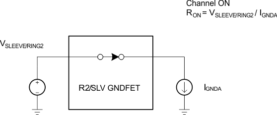 Figure 5. RING2/SLEEVE GNDFET On Resistance Measurement
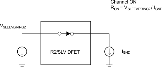 Figure 6. RING2/SLEEVE DFET On Resistance Measurement
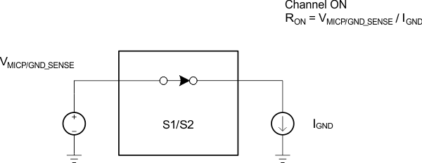 Figure 7. S1/S2 On Resistance Measurement
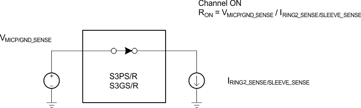 Figure 8. S3PS, S3PR, S3GS, S3GR On Resistance Measurement
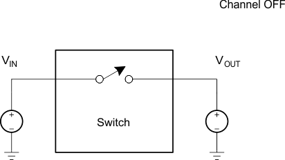 Figure 9. Switch Off Leakage Current
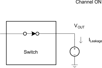 Figure 10. Switch On Leakage Current
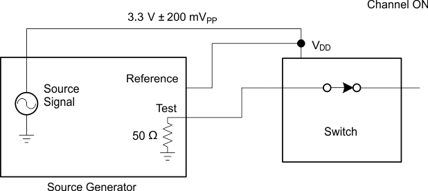 Figure 11. Power Supply Rejection Ratio (PSRR)
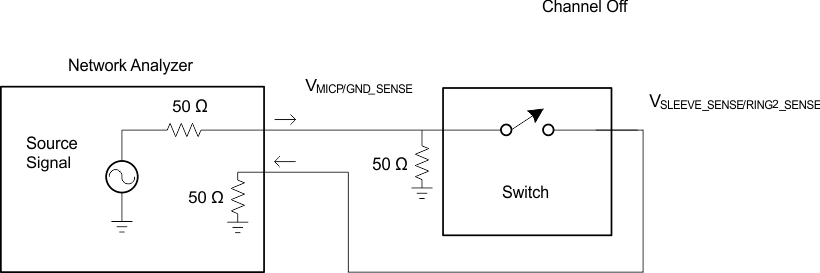 Figure 12. Switch Off Isolation
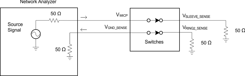 Figure 13. Channel Separation
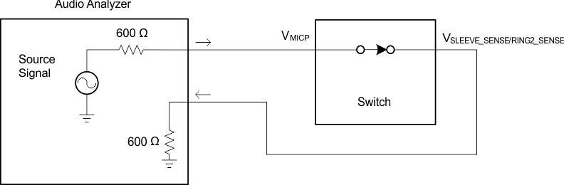 Figure 14. Total Harmonic Distortion (THD) and SNR
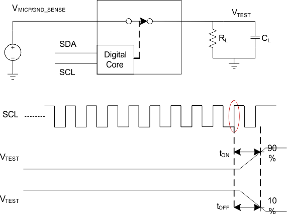 Figure 15. S3 tOFF/tON
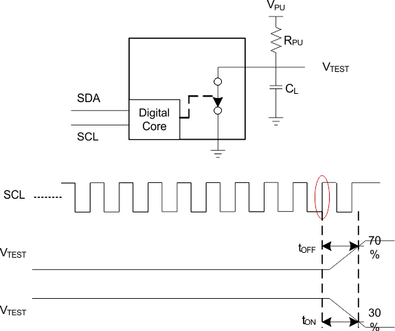 Figure 16. S1, S2, GNDFET and DFET tON/tOFF