SCDS358B November 2014 – February 2015 TS3A227E
PRODUCTION DATA.
- 1 Features
- 2 Applications
- 3 Description
- 4 Simplified Schematic
- 5 Revision History
- 6 Pin Configuration and Functions
- 7 Specifications
- 8 Parameter Measurement Information
-
9 Detailed Description
- 9.1 Overview
- 9.2 Functional Block Diagram
- 9.3 Feature Description
- 9.4 Device Functional Modes
- 9.5 Register Maps
- 9.6
Register Field Descriptions
- 9.6.1 Device ID Register Field Descriptions (Address 00h)
- 9.6.2 Interrupt Register Field Descriptions (Address 01h)
- 9.6.3 Key Press Interrupt Register Field Descriptions (Address 02h)
- 9.6.4 Interrupt Disable Register Field Descriptions (Address 03h)
- 9.6.5 Device Settings Field Descriptions (Address 04h)
- 9.6.6 Key Press Settings 1 Field Descriptions (Address 05h)
- 9.6.7 Key Press Settings 2 Field Descriptions (Address 06h)
- 9.6.8 Switch Control 1 Field Descriptions (Address 07h)
- 9.6.9 Switch Control 2 Field Descriptions (Address 08h)
- 9.6.10 Switch Status 1 Field Descriptions (Address 09h)
- 9.6.11 Switch Status 2 Field Descriptions (Address 0Ah)
- 9.6.12 Detection Results Field Descriptions (Address 0Bh)
- 9.6.13 ADC Output Field Descriptions (Address 0Ch)
- 9.6.14 Threshold 1 Field Descriptions (Address 0Dh)
- 9.6.15 Threshold 2 Field Descriptions (Address 0Eh)
- 9.6.16 Threshold 3 Field Descriptions (Address 0Fh)
- 10Application and Implementation
- 11Power Supply Recommendations
- 12Layout
- 13Device and Documentation Support
- 14Mechanical, Packaging, and Orderable Information
Package Options
Mechanical Data (Package|Pins)
Thermal pad, mechanical data (Package|Pins)
Orderable Information
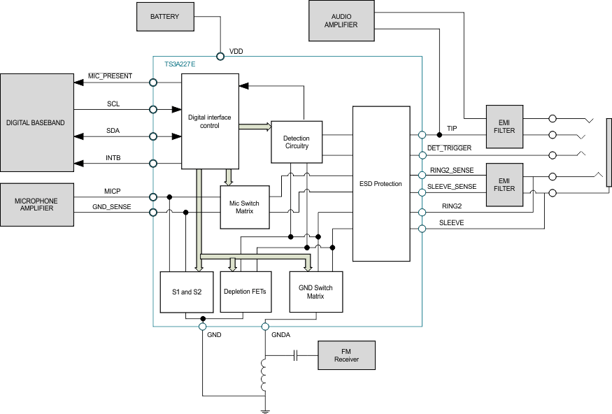
9 Detailed Description
9.1 Overview
The TS3A227E is an autonomous audio accessory switch with adjustable de-bounce settings, ultra-low RON ground FETs, depletion FETs and manual I2C control.
The detection sequence is initiated via the external DET_TRIGGER pin or via I2C command. The device incorporates internal de-bounce timings that remove the need for external RC circuits, reducing cost and overall PCB footprint. Additionally all switches of the TS3A227E and the internal de-bounce timings can be controlled through I2C.
Before an insertion, TS3A227E isolates the MICBIAS voltage output from the audio jack to remove click/pop noise that can be created during an insertion event. In addition the device also includes depletion FETs to ground the accessory SLEEVE and RING2 pins when VDD is not powered. This removes the humming noise that can be created when plugging an accessory into and unpowered system.
The TS3A227E detects the presence and configuration of the microphone in an attached headset upon insertion. Upon detection of a microphone the TS3A227E automatically connects a system analog microphone pin (MICP) to the appropriate audio jack connection. The device also automatically routes the device GNDA pin to the headset ground. After a 4-pole headset insertion the host can enable the Key Press detection feature of the TS3A227E.
The device also features an ultra-low power sleep mode to conserve battery life when an accessory is not inserted.
For FM transmission the ground FETs of the device can be used as an FM transmission path by placing the FM receiver and matching network on the GNDA pin. The FM support bit must be set to ‘1’ through I2C for FM transmission to pass.
9.2 Functional Block Diagram
9.3 Feature Description
9.3.1 Accessory Configuration Detection
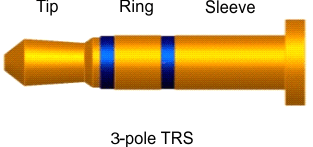
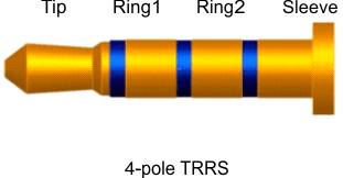
There are currently two difference configurations for headsets with microphones as shown in Table 1. Many codecs requires that the system designer make a tough decision via a hardware connection which headset they would like to support. This is done by directly connecting the microphone bias and the ground connections to the sleeve and ring2 pins of the audio jack. For the end user this leaves a headset standard as fully unsupported.
Table 1. Two Difference Configurations for Headsets
| PHYSICAL CONNECTOR | INTERNAL IMPEDANCE NETWORK | PIN NAME | CONFIGURATION |
|---|---|---|---|
 |
 |
Tip | Audio Left |
| Ring | Audio Right | ||
| Sleeve | Ground | ||
 |
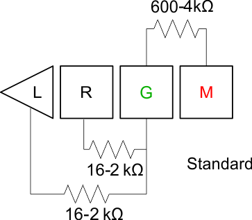 |
Tip | Audio Left |
| Ring1 | Audio Right | ||
| Ring2 | Ground | ||
| Sleeve | Microphone | ||
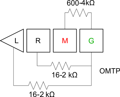 |
Tip | Audio Left | |
| Ring1 | Audio Right | ||
| Ring2 | Microphone | ||
| Sleeve | Ground |
The TS3A227E fills this system gap by detecting the presence and location of the microphone and automatically routing the MICBIAS and ground lines to support each headset. This enhances the overall user experience by allowing headsets from all manufacturers.
9.3.2 Optional Manual I2C Control
The TS3227E also features optional manual I2C control for enhanced system flexibility. This allows the system designer to manually control the switches and de-bounce settings at their discretion enabling the TS3A227E to adapt to unique use cases.
This is an optional feature that does not need to be used for the device to operate autonomously.
9.3.3 Adjustable De-bounce Timings
The TS3A227E features manual control of the insertion de-bounce timer with selectable values. The default insertion de-bounce timer is 90 ms.
This eliminates the need for external RC components which reduces BOM cost, the PCB footprint of the external RC components. Further information on how to select an appropriate de-bounce timer can be found in the application and implementation section.
9.3.4 Key Press Detection
After a headset is inserted, the host can enable Key Press detection through the I2C registers. This will configure the TS3A227E to detect up to 4 different keys and report when the key is pressed and released.
9.3.5 Click Pop Noise Reduction
During an accessory insertion and removal event the TS3A227E use special techniques to remove the click/pop noise that can occur with a traditional implementation creating a better user experience.
9.3.6 Power off Noise Removal
In a system that intends to support both headset types, the end user can place the system into sleep mode and leave a headset/speaker plugged into the audio jack. If the audio jack switch is turned off to conserve power in the sleep mode this would typically mean the headset/speaker ground would not be connected because there is no power to turn on the ground FETs. This creates an audible humming noise at the speaker/headset output that can be discomforting to listen to.
By utilizing always on depletion FETs this issue can be removed and the headset/speaker can be connected to ground even with the device unpowered.
9.3.7 Sleep Mode
The TS3A227E will automatically enter a low power sleep when no accessory is inserted and manual switch control is not enabled. After an accessory is inserted the device will wake, run detection, and configure the switches as necessary.
9.3.8 Codec Sense Line
In the complex systems of today, there is an increasing amount of ICs on any given board. The issue this creates is that a codec can be far away from the audio jack and there is a potential difference between the grounding of the codec and the grounding of the headset.
By incorporating a ground sense line into the TS3A227E the codec can compensate for this offset and create a higher quality audio experience.
9.3.9 FM Support
FM can be picked up using the headset ground line and passed through the ground FETs of the TS3A227E. By having a bandwidth of 200 MHz the full FM band can be passed through these FETs to a FM matching network and the FM receiver.
9.4 Device Functional Modes
9.4.1 Sleep Mode
The device will realize a sleep mode of 1 µA if the following are true:
- No accessory is inserted
- Manual Switch Control = ‘0’
The TS3A227E will respond to I2C communication and insertion events while in sleep mode. The user can set the de-bounce settings and device configuration as desired while in the sleep mode. If the user sets the Manual Switch Control bit to ‘1’ the device will turn on all blocks and come out of sleep mode.
If there is no accessory inserted and the users exits manual switch control, the switches will revert to the no-insertion state and all unnecessary blocks of the TS3A227E will turn off and enter the sleep mode.
9.4.2 Manual Switch Control
The TS3A227E supports manual switch control that can be utilized by setting Bit6 of the Device Settings 1 register to ‘1’.
Key operational characteristics of manual switch control are below.
- Enabling the manual switch control does not disable automatic insertion and accessory type detection.
- Manual Switch Control is blocked during accessory type detection which includes an automatic detection sequence or a manual SW triggered detection sequence. Any changes to the switch control registers, or setting the device to manual switch control will not update the switches until after the accessory type detection has completed.
- Manual Switch Control is also blocked during de-bounce periods.
- Excluding items 2 and 3 above, immediately after the system enables manual switch control the switch states will change to reflect the switch control registers. It is advised to set the desired state of the switches before enabling manual switch control.
- Turning off the depletion FETs of the device will result in increased power consumption as defined in the electrical characteristics table.
- Immediately upon setting Manual Switch Control = ‘0’ the device will automatically configure the switches to the latest detection state. If an accessory is inserted but the TS3A227E has not run detection due to Auto_Det_EN = ‘0’, the switch status will revert to the no insertion state.
- The device cannot be in sleep mode and utilize manual switch control at the same time.
9.4.3 Manual Switch Control Use Cases
The table below captures what occurs after a 3-pole insertion with the Manual Switch Control, Auto DET Enable, and DET Trigger bits set to the following before an insertion.
| MANUAL SWITCH CONTROL | AUTO DET EN | DET TRIGGER (SW) | DOES TYPE DETECTION RUN | SWITCH STATUS AFTER INSERTION | DET TRIGGER (SW) AFTER INSERTION | |
|---|---|---|---|---|---|---|
| 0 | 0 | 0 | no | No-insertion | 0 | |
| 0 | 0 | 1 | yes | 3-pole config | 0 | |
| 0 | 1 | 0 | yes | 3-pole config | 0 | |
| 0 | 1 | 1 | yes | 3-pole config | 0 | |
| 1 | 0 | 0 | no | Switch control registers | 0 | |
| 1 | 0 | 1 | yes | Switch control registers | 0 | |
| 1 | 1 | 0 | yes | Switch control registers | 0 | |
| 1 | 1 | 1 | yes | Switch control registers | 0 |
The table below captures the switch and relevant register outputs for sequence 1.
| EVENT NO. |
EVENT DESCRIPTION | SWITCH STATUS | 3-POLE BIT |
4-POLE STANDARD BIT | 4-POLE OMTP BIT |
|
|---|---|---|---|---|---|---|
| 1 | Device powers up | No-insertion | 0 | 0 | 0 | |
| 2 | User sets Auto DET Enable = ‘0’ | No-insertion | 0 | 0 | 0 | |
| 3 | 3-pole accessory is inserted | No-insertion | 0 | 0 | 0 | |
| 4 | System sets Manual Switch Control = ‘1’ | System controlled | 0 | 0 | 0 | |
| 5 | System sets switch control registers = 0xFF | System controlled | 0 | 0 | 0 | |
| 6 | System sets Manual Switch Control = ‘0’ | No-insertion | 0 | 0 | 0 |
In sequence 1 at event 3 the switch status does not change because the system set the Auto DET Enable = ‘0’. When the accessory is inserted we will not run detection and not change the switches because of this.
At event 6 the system turns off manual switch control, the switch state reverts back to the No-insertion state because the TS3A227E has not ran detection.
The table below captures the switch and relevant register outputs for sequence 2.
| EVENT NO. |
EVENT DESCRIPTION | SWITCH STATUS AFTER EVENT |
3-POLE BIT |
4-POLE STANDARD BIT |
4-POLE OMTP BIT |
|
|---|---|---|---|---|---|---|
| 1 | Device powers up | No-insertion | 0 | 0 | 0 | |
| 2 | User sets Auto DET Enable = ‘0’ | No-insertion | 0 | 0 | 0 | |
| 3 | 3-pole accessory is inserted | No-insertion | 0 | 0 | 0 | |
| 4 | System sets Manual Switch Control = ‘1’ | System controlled | 0 | 0 | 0 | |
| 5 | System sets switch control registers = 0xFF | System controlled | 0 | 0 | 0 | |
| 6 | System sets DET Trigger = ‘1’ | System controlled | 1 | 0 | 0 | |
| 7 | System sets Manual Switch Control = '0' | 3-pole configuration | 1 | 0 | 0 |
In sequence 2 at event 3 the switch status does not change because the system set the Auto DET Enable = ‘0’. When the accessory is inserted we will not run detection and not change the switches because of this.
At event 6 the system turns triggers a manual type detection and the TS3A227E detects a 3-pole accessory. The switch state will remain in the system controlled state.
At event 7 the system exits manual switch control. The switch status will then change back to the last detection state. Because detection was ran at event 6 and a 3-pole was detected, the switch state will reflect that of the 3-pole switch configuration.
9.4.4 FM Support Mode
FM support mode needs to be entered via I2C through the Device Settings register. This will turn off the depletion switches when an accessory is inserted, eliminating the extra ground path. The ground line of the headset/headphone is used for FM transmission. This signal must pass through the TS3A227E ground FETs as shown in Figure 17 where the red line indicates the transmission path.
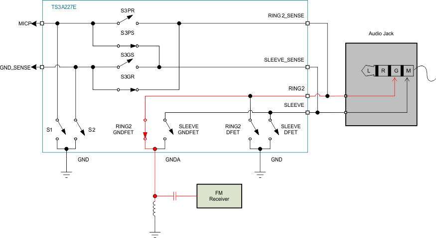 Figure 17. FM Support Transmission Path
NOTE
FM support should be enabled before an accessory is inserted. Toggling the FM support bit after a headset is inserted can cause a pop noise to be heard by the end user.
9.5 Register Maps
The I2C address of the TS3A227E is b’0111011X or 77h read and 76h write.
| Addr (xxh) | Name | Type | Reset | Bit7 | Bit6 | Bit5 | Bit4 | Bit3 | Bit2 | Bit1 | Bit0 |
|---|---|---|---|---|---|---|---|---|---|---|---|
| 00h | Device ID | R | 11h | 0 | 0 | 0 | 1 | 0 | 0 | 0 | 1 |
| 01h | Interrupt | R | 00h | Reserved | ADC Conversion | DC | Ins/Rem Event | ||||
| 02h | Key Press Interrupts | R | 00h | Key 4 Release | Key 4 Press | Key 3 Release | Key 3 Press | Key 2 Release | Key 2 Press | Key 1 Release | Key 1 Press |
| 03h | Interrupt Disable | R/W | 08h | Reserved | INT Disable | ADC Conversion INT Disable | DC INT Disable | Ins/Rem Event INT Disable | |||
| 04h | Device Settings | R/W | 23h | Reset | Manual Switch Control | Auto DET Enable | DET Trigger | FM Support | Insertion De-bounce Time | ||
| 05h | Device Setting 1 | R/W | 00h | Reserved | Key Press Enable | Raw Data En | ADC Trigger | ||||
| 06h | Device Setting 2 | R/W | 0Eh | Reserved | MICBIAS Setting | Key Release De-bounce |
Key Press De-bounce | ||||
| 07h | Switch Control 1 | R/W | 00h | Reserved | SLEEVE GNDFET | RING2 GNDFET |
SLEEVE DFET | RING2 DFET | Switch 2 | Switch 1 | |
| 08h | Switch Control 2 | R/W | 00h | Reserved | S3PS | S3PR | S3GS | S3GR | |||
| 09h | Switch Status 1 | R | 0Ch | Reserved | SLEEVE GNDFET | RING2 GNDFET |
SLEEVE DFET | RING2 DFET | Switch 2 | Switch 1 | |
| 0Ah | Switch Status 2 | R | 00h | Reserved | S3PS | S3PR | S3GS | S3GR | |||
| 0Bh | Accessory Status | R | 00h | Reserved | Insertion Status | 4-Pole Standard | 4-pole OMTP | 3-pole | |||
| 0Ch | ADC Output | R | 00h | ADC | |||||||
| 0Dh | Threshold 1 | R/W | 20h | KP Threshold 1 | |||||||
| 0Eh | Threshold 2 | R/W | 40h | KP Threshold 2 | |||||||
| 0Fh | Threshold 3 | R/W | 68h | KP Threshold 3 | |||||||
Interrupt and Key Press Interrupt register notes:
- The device will continue to automatically run type detection and key press detection even if the host has not serviced the interrupts.
- Consecutive reads of an interrupt register at 400 kHz will not allow time for the internal registers to clear and will appear. The internal digital core requires 200 µs to clear the register after it has been read.
9.6 Register Field Descriptions
9.6.1 Device ID Register Field Descriptions (Address 00h)
| Bit | Field | Type | Reset | Description |
|---|---|---|---|---|
| 7-0 | Device ID | R | 11h | Unique Revision number |
9.6.2 Interrupt Register Field Descriptions (Address 01h)
Table 2. Interrupt Register Field Descriptions (Address 01h)
| Bit | Field | Type | Reset | Description |
|---|---|---|---|---|
| 7-3 | Reserved | R | 0h | |
| 2 | ADC Conversion | R | 0h | ADC Conversion complete Interrupt. Flagged after a manual ADC conversion is complete. |
| Interrupt bit is cleared after being read through I2C or after a removal event. | ||||
| 0h = Default state 1h = ADC Conversion Complete |
||||
| 1 | DC | R | 0h | Detection Complete interrupt. Flagged after detection is completed for an insertion sequence. This bit is also flagged after completion of a manually triggered detection. |
| Interrupt bit is cleared after being read through I2C or after a removal event. | ||||
| 0h = Default state 1h = Detection Completed |
||||
| 0 | Ins/Rem Event | R | 0h | Insertion or removal interrupt indicator. This bit is set if there is an insertion or removal event. The Insertion status bit of the Accessory Status register (0Bh) must be checked if this bit is set. |
| Interrupt bit is cleared after being read through I2C | ||||
| 0h = Default state 1h = Accessory has been inserted or removed |
9.6.3 Key Press Interrupt Register Field Descriptions (Address 02h)
Table 3. Key Press Interrupt Register Field Descriptions (Address 02h)
| Bit | Field | Type | Reset | Description | ||
|---|---|---|---|---|---|---|
| 7 | Key 4 Release | R | 0h | This interrupt bit is set after the user has released key 4 on the accessory for a duration longer than the Key Release De-bounce timer. | ||
| This bit will auto-clear on the following conditions: | ||||||
| ● | Host reads the register through I2C | |||||
| ● | The KP Enable bit is set to ‘0’ | |||||
| — | The KP Enable bit is set to ‘0’ automatically after a removal | |||||
| ● | The Key 4 press bit is set ot '1' | |||||
| 0h = Default State 1h = Key 4 was released |
||||||
| 6 | Key 4 Press | R | 0h | This interrupt bit is set after the user has pressed key 4 on the accessory for a duration longer than the Key Press De-bounce timer. | ||
| This bit will auto-clear on the following conditions: | ||||||
| ● | Host reads the register through I2C | |||||
| ● | The KP Enable bit is set to ‘0’ | |||||
| — | The KP Enable bit is set to ‘0’ automatically after a removal | |||||
| 0h = Default State 1h = Key 4 was released |
||||||
| 5 | Key 3 Release | R | 0h | This interrupt bit is set after the user has pressed Key 3 on the accessory for a duration longer than the Key Release De-bounce timer. | ||
| This bit will auto-clear on the following conditions: | ||||||
| ● | Host reads the register through I2C | |||||
| ● | The KP Enable bit is set to ‘0’ | |||||
| — | The KP Enable bit is set to ‘0’ automatically after a removal | |||||
| ● | The Key 3 Press bit is set to ‘1’ | |||||
| 0h = Default State 1h = Key 3 was released |
||||||
| 4 | Key 3 Press | R | 0h | This interrupt bit is set after the user has pressed Key 3 on the accessory for a duration longer than the Key Press De-bounce timer. | ||
| This bit will auto-clear on the following conditions: | ||||||
| ● | Host reads the register through I2C | |||||
| ● | The KP Enable bit is set to ‘0’ | |||||
| — | The KP Enable bit is set to ‘0’ automatically after a removal | |||||
| 0h = Default State 1h = Key 3 was released |
||||||
| 3 | Key 2 Release | R | 0h | This interrupt bit is set after the user has pressed Key 2 on the accessory for a duration longer than the Key Release De-bounce timer. | ||
| This bit will auto-clear on the following conditions: | ||||||
| ● | Host reads the register through I2C | |||||
| ● | The KP Enable bit is set to ‘0’ | |||||
| — | The KP Enable bit is set to ‘0’ automatically after a removal | |||||
| ● | The Key 2 Press bit is set to ‘1’ | |||||
| 0h = Default State 1h = Key 2 was released |
||||||
| 2 | Key 2 Press | R | 0h | This interrupt bit is set after the user has pressed Key 2 on the accessory for a duration longer than the Key Press De-bounce timer. | ||
| This bit will auto-clear on the following conditions: | ||||||
| ● | Host reads the register through I2C | |||||
| ● | The KP Enable bit is set to ‘0’ | |||||
| — | The KP Enable bit is set to ‘0’ automatically after a removal | |||||
| 0h = Default State 1h = Key 2 was released |
||||||
| 1 | Key 1 Release | R | 0h | This interrupt bit is set after the user has pressed Key 1 on the accessory for a duration longer than the Key Release De-bounce timer. This bit is used for raw data release events. | ||
| This bit will auto-clear on the following conditions: | ||||||
| ● | Host reads the register through I2C | |||||
| ● | The KP Enable bit is set to ‘0’ | |||||
| — | The KP Enable bit is set to ‘0’ automatically after a removal | |||||
| ● | The Key 1 Press bit is set to ‘1’ | |||||
| 0h = Default State 1h = Key 1 was released |
||||||
| 0 | Key 1 Press | R | 0h | This interrupt bit is set after the user has pressed Key 1 on the accessory for a duration longer than the Key Press De-bounce timer. This bit is used for raw data press events. | ||
| This bit will auto-clear on the following conditions: | ||||||
| ● | Host reads the register through I2C | |||||
| ● | The KP Enable bit is set to ‘0’ | |||||
| — | The KP Enable bit is set to ‘0’ automatically after a removal | |||||
| 0h = Default State 1h = Key 1 was released |
||||||
9.6.4 Interrupt Disable Register Field Descriptions (Address 03h)
Table 4. Interrupt Disable Register Field Descriptions (Address 03h)
| Bit | Field | Type | Reset | Description |
|---|---|---|---|---|
| 7-3 | Reserved | R | 0h | |
| +3 | INT Disable | R/W | 1h | Enables or disables all interrupts. Disabling the interrupts will cause the INT to not assert but the bits will still populate. 0h = interrupts are enabled 1h = interrupts are disabled |
| 2 | ADC Conversion INT Disable | R/W | 0h | Enables or disables the ADC conversion interrupt. Disabling the interrupt will cause INT to not assert but the interrupt bit will still be set . |
| In the use case that this bit is == ‘1’ and a key is pressed, the Key Press interrupt will still assert the INT pin. If the host issues a software ADC trigger after the key has been pressed, the interrupt will not assert as that ADC conversion is the only interrupt present. 0h = ADC Conversion interrupt is enabled 1h = ADC Conversion interrupt is disabled |
||||
| 1 | DC INT Disable | R/W | 0h | Enables or disables the DC interrupt. Disabling the interrupt will cause INT to not assert but the interrupt bit will still be set. 0h = DC interrupt is enabled 1h = DC interrupt is disabled |
| 0 | Ins/Rem Event INT Disable | R/W | 0h | Enables or disables the Ins/Rem Event interrupt. Disabling the interrupt will cause INT to not assert but the interrupt bit will still be set. 0h = Ins/Rem Event interrupt is enabled 1h = Ins/Rem Event interrupt is disabled |
9.6.5 Device Settings Field Descriptions (Address 04h)
Table 5. Device Settings Field Descriptions (Address 04h)
| Bit | Field | Type | Reset | Description | |
|---|---|---|---|---|---|
| 7 | Reset | R/W | 0h | Initiates software reset of the TS3A227E. This will interrupt any on-going operation internal to the device. 0h = Default state 1h = Initiates a reset |
|
| 6 | Manual Switch Control | R/W | 0h | Enables Manual control of the TS3A227E switches. After enabling manual switch control the switch status will immediately reflect the values in the switch control registers provided accessory type. 0h = Manual switch control disabled 1h = Manual switch control enabled |
|
| 5 | Auto DET Enable | R/W | 1h | Controls whether detection is automatically ran after an insertion. 0h = Auto accessory detection is disabled 1h = Auto accessory detection is enabled |
|
| 4 | DET Trigger | R/W | 0h | Manually triggers detection. This bit is auto cleared after detection is completed. | |
| A DET Trigger request will be ignored in the following cases: | |||||
| ● | A detection event is currently being service. | ||||
| ● | The interrupt register is not cleared (Register 02h must be = 00h) | ||||
| ● | There is no accessory inserted (/DET_TRIGGER is high) | ||||
| 0h = Default value 1h = Manually trigger detection |
|||||
| 3 | FM Support | R/W | 0h | Turns on FM support. This will turn off the depletion FETs if any accessory is inserted allowing FM transmission through the ground FETs at the cost of increased current consumption. 0h = FM not supported and depletion FETs are on after an insertion 1h = FM supported and depletion FETs are off after an insertion |
|
| 2.0 | Insertion De-bounce Time | R/W | 3h | Controls the insertion de-bounce timer. Values below are typical values that have ±30% variation. Values in addition have a ±1 ms variation though this will only really affect the 2 ms timer. 0h = 2 ms 1h = 30 ms 2h = 60 ms 3h = 90 ms 4h = 120 ms 5h = 150 ms 6h = 1 s 7h = 2 s |
|
9.6.6 Key Press Settings 1 Field Descriptions (Address 05h)
Table 6. Device Settings 1 Field Descriptions (Address 05h)
| Bit | Field | Type | Reset | Description | |
|---|---|---|---|---|---|
| 7-3 | Reserved | R | 0h | ||
| 2 | Key Press Enable | R/W | 0h | Enables the Key Press detection of the TSA227E. This bit auto clears after a removal event. | |
| If the Key Press Enable bit is set ‘1’ and the Manual Switch Control bit is set to ‘1’, the S3 matrix must be in one of the two correct position as described in the Key Press Detection section for the TS3A227E to run key press detection. 0h = Default state 1h = Enables Key Press detection |
|||||
| 1 | Raw Data En | R/W | 0h | Enables the Raw data mode for Key Press Detection. This bit auto clears if the Key Press Enable bit is set to ‘0’. | |
| Enabling raw data mode will not clear the KP interrupt register. After enabling Raw Data any key press and release event is recorded using the Key 1 Press and Key 2 Press Release event. The ADC conversion will be recorded in the ADC output register. 0h = Raw Data is not enabled 1h = Raw Data is enabled |
|||||
| 0 | ADC Trigger | R/W | 0h | Causes a manual ADC trigger if the Key Press Enable and Raw Data EN bits are both set to ‘1’. After the ADC conversion is complete the ADC Conversion interrupt will be set and the ADC Output register will be populated. | |
| This bit auto clears after the ADC Conversion is complete. A new ADC Conversion can be initiated even if the ADC Conversion interrupt has not been serviced. 0h = Default State 1h = Triggers ADC conversion |
|||||
9.6.7 Key Press Settings 2 Field Descriptions (Address 06h)
Table 7. Device Settings 2 Field Descriptions (Address 06h)
| Bit | Field | Type | Reset | Description |
|---|---|---|---|---|
| 7-6 | Reserved | R | 0h | |
| 5-3 | MICBIAS Setting | R/W | 1h | This controls the key press threshold. Set this setting closest to the intended MICBIAS voltage |
| 0h = 2.1 V 1h = 2.2 V (Default) 2h = 2.3 V 3h = 2.4 V 4h = 2.5 V 5h = 2.6 V 6h = 2.7 V 7h = 2.8 V |
||||
| 2 | Key Release De-bounce | R/W | 1h | Controls the Key-Release de-bounce timer. Values below are typical values that have ±30% variation. Values in addition have a ±1 ms variation though this will only really affect the 2 ms timer. |
| 0h = 2 ms 1h = 20 ms (Default) |
||||
| 1-0 | Key Press De-bounce | R/W | 2h | Controls the key press de-bounce timer. Values below are typical values that have ±30% variation. Values in addition have a ±1 ms variation though this will only really affect the 2 ms timer. |
| 0h = 2 ms 1h = 40 ms 2h = 80 ms (Default) 3h = 120 ms |
9.6.8 Switch Control 1 Field Descriptions (Address 07h)
Table 8. Switch Control 1 Field Descriptions (Address 07h)
| Bit | Field | Type | Reset | Description |
|---|---|---|---|---|
| 7-6 | Reserved | R | 0h | |
| 5 | SLEEVE GNDFET | R/W | 0h | Configures the state of the SLEEVE GNDFET if manual switch control is enabled. If manual switch control is not enabled this bit is ignored. 0h = SLEEVE GNDFET switch off 1h = SLEEVE GNDFET switch on |
| 4 | RING2 DFET | R/W | 0h | Configures the state of the RING2 GNDFET if manual switch control is enabled. If manual switch control is not enabled this bit is ignored. 0h = RING2 GNDFET switch off 1h = RING2 GNDFET switch on |
| 3 | SLEEVE DFET | R/W | 0h | Configures the state of the SLEEVE DFET if manual switch control is enabled. If manual switch control is not enabled this bit is ignored. 0h = SLEEVE DFET switch off 1h = SLEEVE DFET switch on |
| 2 | RING2 DFET | R/W | 0h | Configures the state of the RING2 DFET if manual switch control is enabled. If manual switch control is not enabled this bit is ignored. 0h = RING2 DFET switch off 1h = RING2 DFET switch on |
| 1 | Switch 2 | R/W | 0h | Configures the state of the Switch 2 if manual switch control is enabled. If manual switch control is not enabled this bit is ignored. 0h = Switch 2 off 1h = Switch 2 on |
| 0 | Switch 1 | R/W | 0h | Configures the state of the Switch 1 if manual switch control is enabled. If manual switch control is not enabled this bit is ignored. 0h = Switch 1 off 1h = Switch 1 on |
9.6.9 Switch Control 2 Field Descriptions (Address 08h)
Table 9. Switch Control 2 Field Descriptions (Address 08h)
| Bit | Field | Type | Reset | Description |
|---|---|---|---|---|
| 7-4 | Reserved | R | 0h | |
| 3 | S3PS | R/W | 0h | Configures the state of the S3PS if manual switch control is enabled. If manual switch control is not enabled this bit is ignored. 0h = S3PS switch off 1h = S3PS switch on |
| 2 | S3PR | R/W | 0h | Configures the state of the S3PR if manual switch control is enabled. If manual switch control is not enabled this bit is ignored. 0h = S3PR switch off 1h = S3PR switch on |
| 1 | S3GS | R/W | 0h | Configures the state of the S3GS if manual switch control is enabled. If manual switch control is not enabled this bit is ignored. 0h = S3GS off 1h = S3GS on |
| 0 | S3GR | R/W | 0h | Configures the state of the S3GR if manual switch control is enabled. If manual switch control is not enabled this bit is ignored. 0h = S3GR off 1h = S3GR on |
9.6.10 Switch Status 1 Field Descriptions (Address 09h)
Table 10. Switch Status 1 Field Descriptions (Address 09h)
| Bit | Field | Type | Reset | Description |
|---|---|---|---|---|
| 7-6 | Reserved | R | 0h | |
| 5 | SLEEVE GNDFET | R | 0h | Indicates the status of SLEEVE GNDFET 0h = SLEEVE GNDFET switch is off 1h = SLEEVE GNDFET switch is on |
| 4 | RING2 GNDFET | R | 0h | Indicates the status of RING2 GNDFET 0h = RING2 GNDFET switch is off 1h = RING2 GNDFET switch is on |
| 3 | SLEEVE DFET | R | 1h | Indicates the status of SLEEVE DFET 0h = SLEEVE DFET switch is off 1h = SLEEVE DFET switch is on |
| 2 | RING2 DFET | R | 1h | Indicates the status of RING2 DFET 0h = RING2 DFET switch is off 1h = RING2 DFET switch is on |
| 1 | Switch 2 | R | 0h | Indicates the status of Switch 2 0h = Switch 2 is off 1h = Switch 2 is on |
| 0 | Switch 1 | R | 0h | Indicates the status of Switch 1 0h = Switch 1 is off 1h = Switch 1 is on |
9.6.11 Switch Status 2 Field Descriptions (Address 0Ah)
Table 11. Switch Status 2 Field Descriptions (Address 0Ah)
| Bit | Field | Type | Reset | Description |
|---|---|---|---|---|
| 7-4 | Reserved | R | 0h | |
| 3 | S3PS | R | 0h | Indicates the status of S3PS 0h = S3PS switch is off 1h = S3PS switch is on |
| 2 | S3PR | R | 0h | Indicates the status of S3PR 0h = S3PR switch is off 1h = S3PR switch is on |
| 1 | S3GS | R | 0h | Indicates the status of S3GS 0h = S3GS is off 1h = S3GS is on |
| 0 | S3GR | R | 0h | Indicates the status of S3GR 0h = S3GR is off 1h = S3GR is on |
9.6.12 Detection Results Field Descriptions (Address 0Bh)
Table 12. Detection Results Field Descriptions (Address 0Bh)
| Bit | Field | Type | Reset | Description |
|---|---|---|---|---|
| 7-4 | Reserved | R | 0h | |
| 3 | Insertion Status | R | 0h | Indicates if an accessory is inserted the jack or not. This bit is set to the corresponding state after an accessory is inserted or removed and should be read after the Ins/Rem Event interrupt has been set to ‘1’. 0h = An accessory is not in the jack 1h = An accessory is in the jack |
| 2 | 4-pole Standard | R | 0h | Indicates if a 4-pole Standard headset is detected. Bit is set after a completed detection sequence. 0h = Default state 1h = 4-pole standard headset detected |
| 1 | 4-pole OMTP | R | 0h | Indicates if a 4-pole OMTP headset is detected. Bit is set after a completed detection sequence. 0h = Default state 1h = 4-pole OMTP headset detected |
| 0 | 3-pole | R | 0h | Indicates if a 3-pole headphone is detected. Bit is set after a completed detection sequence. 0h = Default state 1h = 3-pole headphone detected |
9.6.13 ADC Output Field Descriptions (Address 0Ch)
Table 13. ADC Output Field Descriptions (Address 0Ch)
| Bit | Field | Type | Reset | Description |
|---|---|---|---|---|
| 7-1 | ADC | R/W | 00h | This field contains the output of the key press detection ADC as described in the key press detection register |
| 0 | Reserved | R | 0h |
9.6.14 Threshold 1 Field Descriptions (Address 0Dh)
Table 14. Threshold 1 Field Descriptions (Address 0Dh)
| Bit | Field | Type | Reset | Description |
|---|---|---|---|---|
| 7-01 | KP Threshold 1 | R/W | 20h | This field sets the key 1 and key 2 boundary threshold. This value must always be lower than the Threshold 2 register for proper operation. |
| 0 | Reserved | R | 0h |
9.6.15 Threshold 2 Field Descriptions (Address 0Eh)
Table 15. Threshold 2 Field Descriptions (Address 0Eh)
| Bit | Field | Type | Reset | Description |
|---|---|---|---|---|
| 7-1 | KP Threshold 2 | R/W | 40h | This field sets the key 2 and key 3 boundary threshold. This value must always be lower than the Threshold 3 register and higher than the threshold 2 register for proper operation. |
| 0 | Reserved | R | 0h |
9.6.16 Threshold 3 Field Descriptions (Address 0Fh)
Table 16. Threshold 3 Field Descriptions (Address 0Fh)
| Bit | Field | Type | Reset | Description |
|---|---|---|---|---|
| 7-1 | KP Threshold 3 | R/W | 68h | This field sets the key 3 and key 4 boundary threshold. This value must always be higher than the Threshold 2 register for proper operation. |
| 0 | Reserved | R | 0h |