SLLSEE5D february 2013 – july 2023 TUSB8040A1
PRODUCTION DATA
- 1
- 1Features
- 2Applications
- 3Description
- 4Revision History
- 5Pin Configuration and Functions
- 6Specifications
-
7Detailed Description
- 7.1 Overview
- 7.2 Functional Block Diagram
- 7.3 Memory
- 7.4 I2C EEPROM Operation
- 7.5 SMBus Target Operation
- 7.6
Configuration Registers
- 7.6.1 ROM Signature Register
- 7.6.2 Vendor ID LSB Register
- 7.6.3 Vendor ID MSB Register
- 7.6.4 Product ID LSB Register
- 7.6.5 Product ID MSB Register
- 7.6.6 Device Configuration Register
- 7.6.7 Battery Charging Support Register
- 7.6.8 Device Removable Configuration Register
- 7.6.9 Port Used Configuration Register
- 7.6.10 Reserved Register
- 7.6.11 Reserved Register
- 7.6.12 Language ID LSB Register
- 7.6.13 Language ID MSB Register
- 7.6.14 Serial Number String Length Register
- 7.6.15 Manufacturer String Length Register
- 7.6.16 Product String Length Register
- 7.6.17 Reserved Register
- 7.6.18 Serial Number Registers
- 7.6.19 Manufacturer String Registers
- 7.6.20 Product String Registers
- 7.6.21 Additional Feature Configuration Register
- 7.6.22 Reserved Register
- 7.6.23 Reserved Register
- 7.6.24 Device Status and Command Register
-
8Applications, Implementation, and Layout
- 8.1 Application Information
- 8.2
Typical Application
- 8.2.1 Design Requirements
- 8.2.2
Detailed Design Procedure
- 8.2.2.1 Upstream Port Implementation
- 8.2.2.2 Downstream Port 1 Implementation
- 8.2.2.3 Downstream Port 2 Implementation
- 8.2.2.4 Downstream Port 3 Implementation
- 8.2.2.5 Downstream Port 4 Implementation
- 8.2.2.6 VBUS Power Switch Implementation
- 8.2.2.7 Clock, Reset, I2C/SMBUS, and Misc
- 8.2.2.8 Power Implementation
- 8.2.3 Application Curve
- 8.2.4 Power Supply Recommendations
- 8.2.5
Layout
- 8.2.5.1
Layout Guidelines
- 8.2.5.1.1 Part Placement
- 8.2.5.1.2
Board Layout Considerations
- 8.2.5.1.2.1 RKM Package – QFN (Quad Flat No-Lead)
- 8.2.5.1.2.2 Impedance
- 8.2.5.1.2.3 Critical Signals
- 8.2.5.1.2.4 Crystal
- 8.2.5.1.2.5 USB Interface
- 8.2.5.1.2.6 Differential Pair Signals
- 8.2.5.1.2.7 Port Connectors
- 8.2.5.1.2.8 Reset Terminals
- 8.2.5.1.2.9 Miscellaneous Terminals
- 8.2.5.1.2.10 Power Control and Battery Charging Terminals
- 8.2.5.1.2.11 USB 2.0 Port Indicator LED Terminals
- 8.2.5.1.3 Power
- 8.2.5.2 Layout Example
- 8.2.5.1
Layout Guidelines
- 9Device and Documentation Support
- Mechanical, Packaging, and Orderable Information
Package Options
Mechanical Data (Package|Pins)
- RKM|100
Thermal pad, mechanical data (Package|Pins)
- RKM|100
Orderable Information
8.2.5.1.2.6 Differential Pair Signals
Notes on routing differential pair signals:
- Minimize the trace lengths of the differential pair traces. The maximum recommended trace length for SS differential pair signals and USB 2.0 differential pair signals is eight inches. Longer trace lengths require careful routing to assure proper signal integrity.
- Match the etch lengths of the differential pair traces (that is, DP and DM or SSRXP and SSRXM or SSTXP and SSTXM). There should be less than 5 mils difference between a SS differential pair signal and its complement. The USB 2.0 differential pairs should not exceed 50 mils relative trace length difference.
- Route the differential pair traces parallel to one another and close together as much as possible. The traces should be symmetrical.
- The etch lengths of the differential pair groups do not need to match (that is, the length of the SSRX pair to that of the SSTX pair), but all trace lengths should be minimized.
Note:
To minimize crosstalk, the spacing between the TX and RX signal pairs for each interface should be five times the width of the trace (5W rule). For instance, on the TUSB8040A1 EVM there are 27.5 mils of space between the TX and RX differential pairs. If this 5W rule cannot be implemented, then the space between the TX and RX differential pairs should be maximized as much as possible and ground-fill should be placed between the two. In this case, it is better to route each differential pair on opposite sides of the board with a ground plane between them.
- There should be a general keep-out region of at least 20 mils around the differential pairs so that signals, components, or power/ground planes are not routed close to the differential pairs. The exception is at the TUSB8040A1.
- Minimize the use of vias in the differential pair paths as much as possible. If this is not practical, ensure that the same via type and placement are used for both signals in a pair. Any vias used should be placed as close to the TUSB8040A1 as possible.
- Do not place power fuses across the differential pair traces.
- It is preferable to route the differential pair signals directly from the port to the via under the TUSB8040A1. On the TUSB8040A1 EVM, the differential pair signals “fly-by” the ESD protection devices so that no stubs are created. Depending on board layout, this may not always be possible.
- The differential pairs should be routed over a solid ground plane. This ground plane should run under the entire trace length from the TUSB8040A1 (or via) to the pins of the USB connectors and extend past the traces by 10 mils. Avoid routing differential pairs at 90° angles over power plane edges.
- To ease routing, the polarity of the SS differential pairs can be swapped. Thus SSTXP can be routed to SSTXM, or SSRXM can be routed to SSRXP.
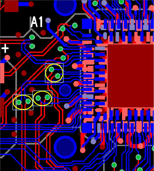
- To route the differential pairs of the TUSB8040A1 to the USB connectors, it is necessary on the downstream ports to cross the SSTX pair and the SSRX pair. To avoid using multiple sets of vias, these were carefully placed on the TUSB8040A1 EVM so that the crossover was inherent in the board design, and both pairs of signals (along with the USB 2.0 differential pair) were routed on the bottom layer.
 Figure 8-20 Using Via Placement to Cross the SSTX and SSRX Pairs