SLLSEE5D february 2013 – july 2023 TUSB8040A1
PRODUCTION DATA
- 1
- 1Features
- 2Applications
- 3Description
- 4Revision History
- 5Pin Configuration and Functions
- 6Specifications
-
7Detailed Description
- 7.1 Overview
- 7.2 Functional Block Diagram
- 7.3 Memory
- 7.4 I2C EEPROM Operation
- 7.5 SMBus Target Operation
- 7.6
Configuration Registers
- 7.6.1 ROM Signature Register
- 7.6.2 Vendor ID LSB Register
- 7.6.3 Vendor ID MSB Register
- 7.6.4 Product ID LSB Register
- 7.6.5 Product ID MSB Register
- 7.6.6 Device Configuration Register
- 7.6.7 Battery Charging Support Register
- 7.6.8 Device Removable Configuration Register
- 7.6.9 Port Used Configuration Register
- 7.6.10 Reserved Register
- 7.6.11 Reserved Register
- 7.6.12 Language ID LSB Register
- 7.6.13 Language ID MSB Register
- 7.6.14 Serial Number String Length Register
- 7.6.15 Manufacturer String Length Register
- 7.6.16 Product String Length Register
- 7.6.17 Reserved Register
- 7.6.18 Serial Number Registers
- 7.6.19 Manufacturer String Registers
- 7.6.20 Product String Registers
- 7.6.21 Additional Feature Configuration Register
- 7.6.22 Reserved Register
- 7.6.23 Reserved Register
- 7.6.24 Device Status and Command Register
-
8Applications, Implementation, and Layout
- 8.1 Application Information
- 8.2
Typical Application
- 8.2.1 Design Requirements
- 8.2.2
Detailed Design Procedure
- 8.2.2.1 Upstream Port Implementation
- 8.2.2.2 Downstream Port 1 Implementation
- 8.2.2.3 Downstream Port 2 Implementation
- 8.2.2.4 Downstream Port 3 Implementation
- 8.2.2.5 Downstream Port 4 Implementation
- 8.2.2.6 VBUS Power Switch Implementation
- 8.2.2.7 Clock, Reset, I2C/SMBUS, and Misc
- 8.2.2.8 Power Implementation
- 8.2.3 Application Curve
- 8.2.4 Power Supply Recommendations
- 8.2.5
Layout
- 8.2.5.1
Layout Guidelines
- 8.2.5.1.1 Part Placement
- 8.2.5.1.2
Board Layout Considerations
- 8.2.5.1.2.1 RKM Package – QFN (Quad Flat No-Lead)
- 8.2.5.1.2.2 Impedance
- 8.2.5.1.2.3 Critical Signals
- 8.2.5.1.2.4 Crystal
- 8.2.5.1.2.5 USB Interface
- 8.2.5.1.2.6 Differential Pair Signals
- 8.2.5.1.2.7 Port Connectors
- 8.2.5.1.2.8 Reset Terminals
- 8.2.5.1.2.9 Miscellaneous Terminals
- 8.2.5.1.2.10 Power Control and Battery Charging Terminals
- 8.2.5.1.2.11 USB 2.0 Port Indicator LED Terminals
- 8.2.5.1.3 Power
- 8.2.5.2 Layout Example
- 8.2.5.1
Layout Guidelines
- 9Device and Documentation Support
- Mechanical, Packaging, and Orderable Information
Package Options
Mechanical Data (Package|Pins)
- RKM|100
Thermal pad, mechanical data (Package|Pins)
- RKM|100
Orderable Information
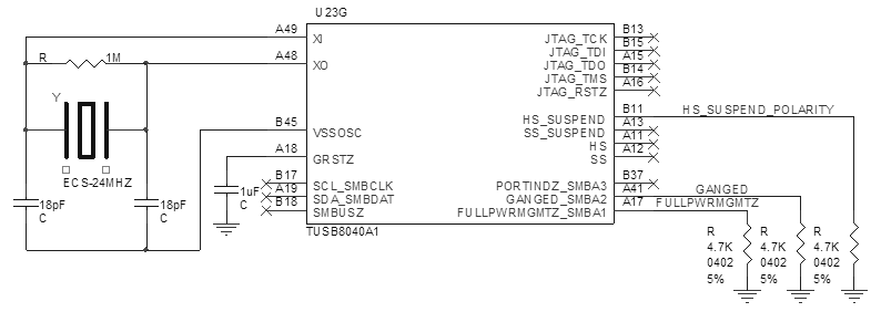
8.2.2.7 Clock, Reset, I2C/SMBUS, and Misc
 Figure 8-8 Clock, Reset, I2C/SMBUS, and Misc
The HS_SUSPEND is pulled-down, which results in active low power enable (PWRON0z, PWRON1z, PWRON2z, and PWRON3z) for a USB VBUS power switch. The 1 μF capacitor on the GRSTZ pin can only be used if the VDD11 supply is stable before the VDD33 supply. The capacitor may need to be adjusted, depending on the power ramp of the two supplies. Also, the GANGED pin and FULLPWRMGMTZ pin are pulled low, resulting in individual power support for each downstream port. Additionally, this particular implementation has the I2C/SMBUS and JTAG interfaces disabled, thus all terminals related to them are left unconnected.