SLUSD48C July 2018 – March 2022 UCC24624
PRODUCTION DATA
- 1 Features
- 2 Applications
- 3 Description
- 4 Revision History
- 5 Description, Continued
- 6 Pin Configuration and Functions
- 7 Specifications
- 8 Detailed Description
- 9 Application and Implementation
- 10Power Supply Recommendations
- 11Layout
- 12Device and Documentation Support
Package Options
Mechanical Data (Package|Pins)
- D|8
Thermal pad, mechanical data (Package|Pins)
Orderable Information
8.3.2 Synchronous Rectifier Control
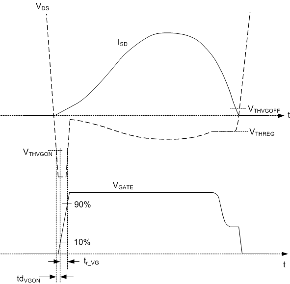
The UCC24624 SR controller determines the conduction time of the SR-MOSFET by comparing the drain-to-source voltage of the MOSFET against a turn-on threshold and a turn-off threshold. The gate driver output is driven high when the VDS of the MOSFET becomes more negative than VTHVGON and is driven low when VDS becomes more positive than VTHVGOFF as illustrated in Figure 8-4.
 Figure 8-4 SR Operation Principle
Note that before SR MOSFET turns on, there is a small delay caused by the internal comparator delay and the gate driver delay. During the delay time, the SR MOSFET body diode is conducting. For LLC resonant converters, this delay is essential for appropriate operation. Due to the large junction capacitors of the SR MOSFETs, the SR often sees a leading-edge current spike early in the conduction period, follow by the real conduction current. Normally, a prolonged minimum on time can override this spike to make the circuit operate normally. However, this causes large negative current that transfer the energy from the output to the input and reduces the overall converter efficiency. In UCC24624, 155-ns turn-on delay is added, to help ignore the leading edge spike.
When the SR MOSFET body diode is conducting, VD pin becomes negative relative to the VSS pin by the body diode drop. The VD and VSS pins must be connected directly to the SR MOSFET pins to avoid any overlapping of sensing paths to the power path and minimize the negative voltage and ringing caused by parasitic inductance. Low package inductance MOSFETs, such as in SON package, are preferred to minimize this effect as well.
Besides the simple comparator, UCC24624 also includes a proportional gate drive feature. For many SR controllers, the SR MOSFET is turned on with the full driving voltage. In this way, the conduction loss can be minimized. However, this method has a few major drawbacks. Because the turn-off threshold is a fixed value, often to prevent negative current, the SR is turned off before the current reaches zero. This causes some SR MOSFET body diode conduction time and increases the conduction loss. Another issue is associated with the LLC converter operating above the resonant frequency. When the converter operates above the resonant frequency, the SR current slope (di/dt) at turn-off could be as high as 150 A/μs. This high current slope could cause negative current if the SR controller has long turn-off propagation delays. Furthermore, the time to discharge the SR MOSFET gate voltage from its full driving voltage to its threshold level introduces another delay. This further increases the negative current.
Instead of always keeping the SR MOSFET on with the full gate-drive voltage, UCC24624 reduces its gate-drive voltage when the voltage drop across the SR MOSFET drain to source becomes more than –35 mV (less negative, closer to zero when current approaching zero). During this time, UCC24624 reduces its gate drive voltage from 11 V to close to the SR MOSFET's threshold voltage, and tries to regulate the SR MOSFET VDS voltage to –35 mV (VTHPGD_LO). This brings two major benefits to the application: a) Preventing the SR premature turn off, which causes extra loss associated with body diode conduction b) Shorter turn-off delay since the SR MOSFET gate voltage is already reduced close to the MOSFET threshold voltage level and the SR MOSFET can be turned off with virtually no delay.
The SR MOSFET is only driven high with its full driving capability of 1.5 A during the gate driver minimum pull-up time tMGPU. After that, the SR MOSFET gate is kept high by a weak current source of approximately 200 µA. Keep the resistor between the SR MOSFET gate and source larger than 100 kΩ to ensure the full driving voltage and a minimized conduction loss.
Due to the sinusoidal current shape in the secondary side SR MOSFETs in an LLC resonant converter, the proportional gate drive could start to reduce the SR gate voltage even at the current rising edge. This increases the conduction loss and reduces the converter efficiency. In UCC24624, the proportional gate drive is disabled during the first half of the SR conduction time, based on the previous cycle's SR conduction time. Therefore, the gate drive voltage is only reduced during the SR current falling edge and this helps to maintain the low conduction loss. The gate drive voltage is forced to reduce if the SR voltage drop does not reach the proportional gate-drive threshold VTHPGD_LO within the 90% of the previous cycle on time. And the proportional gate drive now tries to regulate the VDS to –100 mV (VTHPGD_HI). This further ensures the fast turn-off speed for high di/dt conditions.
To prevent the SR MOSFET premature turn off caused by the large package inductance, an offset resistor can be added between the VSS pin and the SR MOSFET source pins to further increase the turn off threshold. See below section for the details of choosing the resistor value.