SLUSD48C July   2018  – March 2022 UCC24624

PRODUCTION DATA  

  1. Features
  2. Applications
  3. Description
  4. Revision History
  5. Description, Continued
  6. Pin Configuration and Functions
    1.     Pin Functions
  7. Specifications
    1. 7.1 Absolute Maximum Ratings
    2. 7.2 ESD Ratings
    3. 7.3 Recommended Operating Conditions
    4. 7.4 Thermal Information
    5. 7.5 Electrical Characteristics
    6. 7.6 Timing Requirements
    7. 7.7 Typical Characteristics
  8. Detailed Description
    1. 8.1 Overview
    2. 8.2 Functional Block Diagram
    3. 8.3 Feature Description
      1. 8.3.1 Power Management
      2. 8.3.2 Synchronous Rectifier Control
      3. 8.3.3 Turn-off Threshold Adjustment
      4. 8.3.4 Noise Immunity
        1. 8.3.4.1 On-Time Blanking
        2. 8.3.4.2 Off-Time Blanking
        3. 8.3.4.3 Two-Channel Interlock
        4. 8.3.4.4 SR Turn-on Re-arm
        5. 8.3.4.5 Adaptive Turn-on Delay
      5. 8.3.5 Gate Voltage Clamping
      6. 8.3.6 Standby Mode
    4. 8.4 Device Functional Modes
      1. 8.4.1 UVLO Mode
      2. 8.4.2 Standby Mode
      3. 8.4.3 Run Mode
  9. Application and Implementation
    1. 9.1 Application Information
    2. 9.2 Typical Application
      1. 9.2.1 Design Requirements
      2. 9.2.2 Detailed Design Procedure
        1. 9.2.2.1 MOSFET Selection
        2. 9.2.2.2 Snubber Design
      3. 9.2.3 Application Curves
  10. 10Power Supply Recommendations
  11. 11Layout
    1. 11.1 Layout Guidelines
    2. 11.2 Layout Example
  12. 12Device and Documentation Support
    1. 12.1 Device Support
      1. 12.1.1 Development Support
        1. 12.1.1.1 Custom Design With WEBENCH® Tools
    2. 12.2 Receiving Notification of Documentation Updates
    3. 12.3 Community Resources
    4. 12.4 Trademarks

Package Options

Mechanical Data (Package|Pins)
Thermal pad, mechanical data (Package|Pins)
Orderable Information

Typical Application

The UCC24624EVM-015 was used to replace rectifier diodes in a 120-W LLC converter using the UCC256302 LLC controller. The power converter had an input voltage (VIN) range of 340 V to 410 V with a typical input of 390 V, with a regulated 12-V output. More details about this power stage can be found in UCC256301 LLC Evaluation Module. More information regarding designing PFC and LLC stages can be found on these training topics (LLC Design Principles and Optimization for Transient Response, A new way to PFC and an even better way to LLC, and PFC for not dummies).

The schematic of the UCC24624EVM-15 is shown in Figure 9-1.
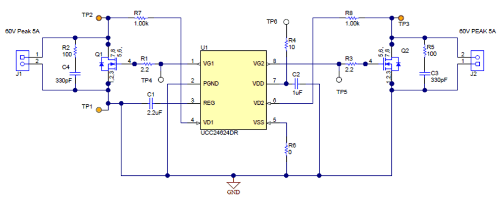
GUID-EF4D93A4-C30C-46A0-9532-CC04707F7529-low.gifFigure 9-1 Schematic of UCC24624EVM-15

The top and bottom view of UCC24624EVM-015 are shown in Figure 11-2 and Figure 11-3.