SGLS121E July   2002  – April 2025 UCC2800-Q1 , UCC2801-Q1 , UCC2802-Q1 , UCC2803-Q1 , UCC2804-Q1 , UCC2805-Q1

PRODUCTION DATA  

  1.   1
  2. Features
  3. Applications
  4. Description
  5. Device Comparison
  6. Pin Configuration and Functions
  7. Specifications
    1. 6.1 Absolute Maximum Ratings
    2. 6.2 ESD Ratings
    3. 6.3 Recommended Operating Conditions
    4. 6.4 Thermal Information
    5. 6.5 Electrical Characteristics
    6. 6.6 Typical Characteristics
  8. Detailed Description
    1. 7.1 Overview
    2. 7.2 Functional Block Diagram
    3. 7.3 Feature Description
      1. 7.3.1  Detailed Pin Description
        1. 7.3.1.1 COMP
        2. 7.3.1.2 FB
        3. 7.3.1.3 CS
        4. 7.3.1.4 RC
        5. 7.3.1.5 GND
        6. 7.3.1.6 OUT
        7. 7.3.1.7 VCC
        8. 7.3.1.8 Pin 8 (REF)
      2. 7.3.2  Undervoltage Lockout (UVLO)
      3. 7.3.3  Self-Biasing, Active Low Output
      4. 7.3.4  Reference Voltage
      5. 7.3.5  Oscillator
      6. 7.3.6  Synchronization
      7. 7.3.7  PWM Generator
      8. 7.3.8  Minimum Off-Time Setting (Dead-Time Control)
      9. 7.3.9  Leading Edge Blanking
      10. 7.3.10 Minimum Pulse Width
      11. 7.3.11 Current Limiting
      12. 7.3.12 Overcurrent Protection and Full Cycle Restart
      13. 7.3.13 Soft Start
      14. 7.3.14 Slope Compensation
    4. 7.4 Device Functional Modes
      1. 7.4.1 Normal Operation
      2. 7.4.2 UVLO Mode
      3. 7.4.3 Soft Start Mode
      4. 7.4.4 Fault Mode
  9. Application and Implementation
    1. 8.1 Application Information
    2. 8.2 Typical Application
      1. 8.2.1 Design Requirements
      2. 8.2.2 Detailed Design Procedure
        1. 8.2.2.1 Current Sensing Network
        2. 8.2.2.2 Gate Drive Resistor
        3. 8.2.2.3 Vref Capacitor
        4. 8.2.2.4 RTCT
        5. 8.2.2.5 Start-Up Circuit
        6. 8.2.2.6 Voltage Feedback Compensation
          1. 8.2.2.6.1 Power Stage Gain, Zeroes, and Poles
          2. 8.2.2.6.2 Compensation Loop
      3. 8.2.3 Application Curves
    3. 8.3 Power Supply Recommendations
    4. 8.4 Layout
      1. 8.4.1 Layout Guidelines
      2. 8.4.2 Layout Example
  10. Device and Documentation Support
    1. 9.1 Related Links
    2. 9.2 Receiving Notification of Documentation Updates
    3. 9.3 Support Resources
    4. 9.4 Trademarks
    5. 9.5 Electrostatic Discharge Caution
    6. 9.6 Glossary
  11. 10Revision History
  12. 11Mechanical, Packaging, and Orderable Information

Package Options

Refer to the PDF data sheet for device specific package drawings

Mechanical Data (Package|Pins)
  • D|8
Thermal pad, mechanical data (Package|Pins)
Orderable Information

Typical Characteristics

UCC2800-Q1 UCC2801-Q1 UCC2802-Q1 UCC2803-Q1 UCC2804-Q1 UCC2805-Q1 Error Amplifier Gain and Phase Response
Figure 6-1 Error Amplifier Gain and Phase Response
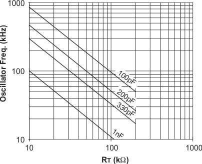
UCC2800-Q1 UCC2801-Q1 UCC2802-Q1 UCC2803-Q1 UCC2804-Q1 UCC2805-Q1 UCC2800-Q1, UCC2801-Q1, UCC2802-Q1, and UCC2804-Q1 Oscillator Frequency vs RT and CT
Figure 6-3 UCC2800-Q1, UCC2801-Q1, UCC2802-Q1, and UCC2804-Q1 Oscillator Frequency vs RT and CT
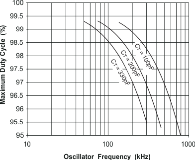
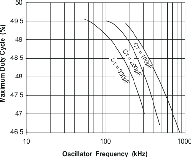
UCC2800-Q1 UCC2801-Q1 UCC2802-Q1 UCC2803-Q1 UCC2804-Q1 UCC2805-Q1 UCC2800-Q1, UCC2802-Q1, and UCC2803-Q1 Maximum Duty Cycle vs Oscillator Frequency
Figure 6-5 UCC2800-Q1, UCC2802-Q1, and UCC2803-Q1 Maximum Duty Cycle vs Oscillator Frequency
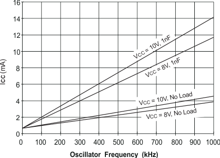
UCC2800-Q1 UCC2801-Q1 UCC2802-Q1 UCC2803-Q1 UCC2804-Q1 UCC2805-Q1 UCC2800-Q1 ICC vs Oscillator Frequency
Figure 6-7 UCC2800-Q1 ICC vs Oscillator Frequency
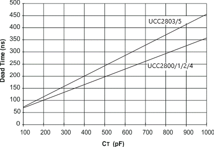
UCC2800-Q1 UCC2801-Q1 UCC2802-Q1 UCC2803-Q1 UCC2804-Q1 UCC2805-Q1 Dead Time vs CT, RT = 100 k
Figure 6-9 Dead Time vs CT, RT = 100 k
UCC2800-Q1 UCC2801-Q1 UCC2802-Q1 UCC2803-Q1 UCC2804-Q1 UCC2805-Q1 Vref vs TemperatureFigure 6-11 Vref vs Temperature
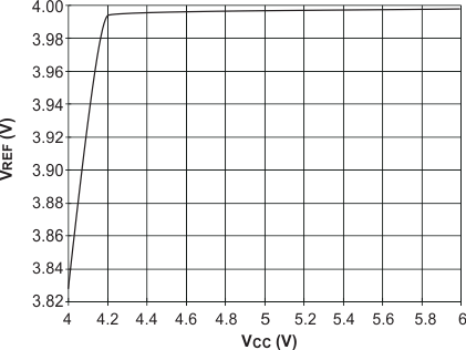
UCC2800-Q1 UCC2801-Q1 UCC2802-Q1 UCC2803-Q1 UCC2804-Q1 UCC2805-Q1 UCC2803-Q1 and UCC2805-Q1VREF vs VCC, ILOAD = 0.5 mA
Figure 6-2 UCC2803-Q1 and UCC2805-Q1VREF vs VCC, ILOAD = 0.5 mA
UCC2800-Q1 UCC2801-Q1 UCC2802-Q1 UCC2803-Q1 UCC2804-Q1 UCC2805-Q1 UCC2803-Q1 and UCC2805-Q1 Oscillator Frequency vs RT and CT
Figure 6-4 UCC2803-Q1 and UCC2805-Q1 Oscillator Frequency vs RT and CT
UCC2800-Q1 UCC2801-Q1 UCC2802-Q1 UCC2803-Q1 UCC2804-Q1 UCC2805-Q1 UCC2801-Q1, UCC2804-Q1, and UCC2805-Q1 Maximum Duty Cycle vs Oscillator Frequency
Figure 6-6 UCC2801-Q1, UCC2804-Q1, and UCC2805-Q1 Maximum Duty Cycle vs Oscillator Frequency
UCC2800-Q1 UCC2801-Q1 UCC2802-Q1 UCC2803-Q1 UCC2804-Q1 UCC2805-Q1 UCC2805-Q1 ICC vs Oscillator Frequency
Figure 6-8 UCC2805-Q1 ICC vs Oscillator Frequency
UCC2800-Q1 UCC2801-Q1 UCC2802-Q1 UCC2803-Q1 UCC2804-Q1 UCC2805-Q1 COMP to CS Offset vs Temperature, CS = 0 V
Figure 6-10 COMP to CS Offset vs Temperature, CS = 0 V
UCC2800-Q1 UCC2801-Q1 UCC2802-Q1 UCC2803-Q1 UCC2804-Q1 UCC2805-Q1 Error Amp. Input vs TemperatureFigure 6-12 Error Amp. Input vs Temperature