SLUSC60B December 2017 – October 2019 UCC28064A
PRODUCTION DATA.
- 1 Features
- 2 Applications
- 3 Description
- 4 Revision History
- 5 Description (Continued)
- 6 Pin Configuration and Functions
- 7 Specifications
-
8 Detailed Description
- 8.1 Overview
- 8.2 Functional Block Diagram
- 8.3
Feature Description
- 8.3.1 Principles of Operation
- 8.3.2 Natural Interleaving
- 8.3.3 On-Time Control, Maximum Frequency Limiting, Restart Timer and Input Voltage Feed-Forward compensation
- 8.3.4 Distortion Reduction
- 8.3.5 Zero-Current Detection and Valley Switching
- 8.3.6 Phase Management and Light-Load Operation
- 8.3.7 Burst Mode Operation
- 8.3.8 External Disable
- 8.3.9 Improved Error Amplifier
- 8.3.10 Soft Start
- 8.3.11 Brownout Protection
- 8.3.12 Line Dropout Detection
- 8.3.13 VREF
- 8.3.14 VCC
- 8.3.15
System Level Protections
- 8.3.15.1 Failsafe OVP - Output Over-voltage Protection
- 8.3.15.2 Overcurrent Protection
- 8.3.15.3 Open-Loop Protection
- 8.3.15.4 VCC Undervoltage Lock-Out (UVLO) Protection
- 8.3.15.5 Phase-Fail Protection
- 8.3.15.6 CS - Open, TSET - Open and Short Protection
- 8.3.15.7 Thermal Shutdown Protection
- 8.3.15.8 Fault Logic Diagram
- 8.4 Device Functional Modes
-
9 Application and Implementation
- 9.1 Application Information
- 9.2
Typical Application
- 9.2.1 Design Requirements
- 9.2.2
Detailed Design Procedure
- 9.2.2.1 Custom Design With WEBENCH® Tools
- 9.2.2.2 Inductor Selection
- 9.2.2.3 ZCD Resistor Selection RZA, RZB
- 9.2.2.4 HVSEN
- 9.2.2.5 Output Capacitor Selection
- 9.2.2.6 Selecting RS For Peak Current Limiting
- 9.2.2.7 Power Semiconductor Selection (Q1, Q2, D1, D2)
- 9.2.2.8 Brownout Protection
- 9.2.2.9 Converter Timing
- 9.2.2.10 Programming VOUT
- 9.2.2.11 Voltage Loop Compensation
- 9.2.3 Application Curves
- 10Power Supply Recommendations
- 11Layout
- 12Package Option Addendum
- 13Device and Documentation Support
- 14Mechanical, Packaging, and Orderable Information
Package Options
Mechanical Data (Package|Pins)
- D|16
Thermal pad, mechanical data (Package|Pins)
Orderable Information
8.3.9 Improved Error Amplifier
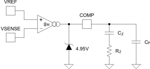
The voltage error amplifier is a transconductance amplifier. Voltage-loop compensation is connected from the error amplifier output, COMP, to analog ground, AGND. The recommended Type-II compensation network is shown in Figure 24. For loop-stability purposes, the compensation network values are calculated based on small-signal perturbations of the output voltage using the nominal transconductance (gain) of 55 µS.
 Figure 24. Transconductance Error Amplifier With Typical Compensation Network
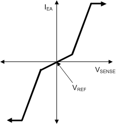
 To improve the transient response to large perturbations, the error amplifier gain increases by a factor of around 5X when the error amplifier input deviates more than ±5% from the nominal regulation voltage, VSENSEreg. This increase allows faster charging and discharging of the compensation components following sudden load-current increases or decreases.
