SLUSBF3D July 2013 – March 2018 UCC28740
PRODUCTION DATA.
- 1 Features
- 2 Applications
- 3 Description
- 4 Revision History
- 5 Pin Configuration and Functions
- 6 Specifications
- 7 Detailed Description
-
8 Application and Implementation
- 8.1 Application Information
- 8.2
Typical Application
- 8.2.1 Design Requirements
- 8.2.2
Detailed Design Procedure
- 8.2.2.1 Custom Design With WEBENCH® Tools
- 8.2.2.2 Standby Power Estimate and No-Load Switching Frequency
- 8.2.2.3 Input Bulk Capacitance and Minimum Bulk Voltage
- 8.2.2.4 Transformer Turns-Ratio, Inductance, Primary Peak Current
- 8.2.2.5 Transformer Parameter Verification
- 8.2.2.6 VS Resistor Divider, Line Compensation
- 8.2.2.7 Output Capacitance
- 8.2.2.8 VDD Capacitance, CVDD
- 8.2.2.9 Feedback Network Biasing
- 8.2.3 Application Curves
- 9 Power Supply Recommendations
- 10Layout
-
11Device and Documentation Support
- 11.1
Device Support
- 11.1.1 Development Support
- 11.1.2
Device Nomenclature
- 11.1.2.1 Capacitance Terms in Farads
- 11.1.2.2 Duty Cycle Terms
- 11.1.2.3 Frequency Terms in Hertz
- 11.1.2.4 Current Terms in Amperes
- 11.1.2.5 Current and Voltage Scaling Terms
- 11.1.2.6 Transformer Terms
- 11.1.2.7 Power Terms in Watts
- 11.1.2.8 Resistance Terms in Ohms
- 11.1.2.9 Timing Terms in Seconds
- 11.1.2.10 Voltage Terms in Volts
- 11.1.2.11 AC Voltage Terms in VRMS
- 11.1.2.12 Efficiency Terms
- 11.2 Documentation Support
- 11.3 Receiving Notification of Documentation Updates
- 11.4 Community Resources
- 11.5 Trademarks
- 11.6 Electrostatic Discharge Caution
- 11.7 Glossary
- 11.1
Device Support
- 12Mechanical, Packaging, and Orderable Information
Package Options
Mechanical Data (Package|Pins)
- D|7
Thermal pad, mechanical data (Package|Pins)
Orderable Information
6.7 Typical Characteristics
VVDD = 25 V, TJ = 25°C, unless otherwise noted.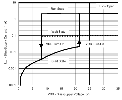
| HV = Open |
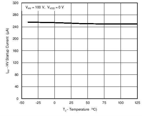
| VHV = 100 V, VVDD = 0 V | ||
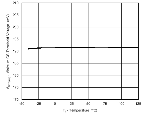 Figure 5. Minimum CS Threshold vs. Temperature
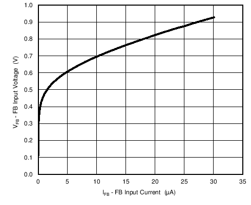 Figure 9. FB Input Voltage vs. FB Input Current
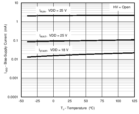
| HV = Open |
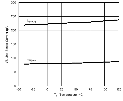
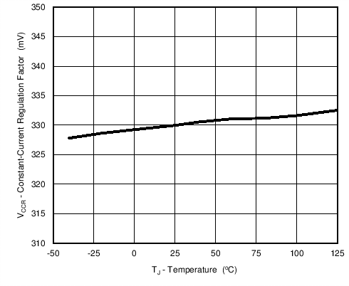 Figure 6. Constant-Current Regulation Factor vs. Temperature
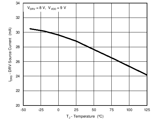
| VDRV = 8 V, VVDD = 9 V | ||
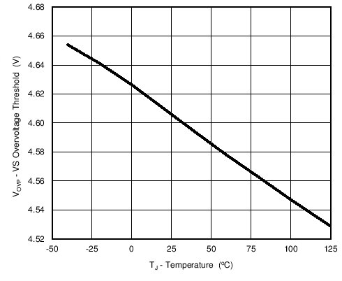 Figure 10. VS Overvoltage Threshold vs. Temperature