SLUSDV5B October 2019 – April 2020 UCC5304
PRODUCTION DATA.
- 1 Features
- 2 Applications
- 3 Description
- 4 Revision History
- 5 Pin Configuration and Functions
-
6 Specifications
- 6.1 Absolute Maximum Ratings
- 6.2 ESD Ratings
- 6.3 Recommended Operating Conditions
- 6.4 Thermal Information
- 6.5 Power Ratings
- 6.6 Insulation Specifications
- 6.7 Safety-Related Certifications
- 6.8 Safety-Limiting Values
- 6.9 Electrical Characteristics
- 6.10 Switching Characteristics
- 6.11 Typical Characteristics
- 7 Parameter Measurement Information
- 8 Detailed Description
- 9 Application and Implementation
- 10Power Supply Recommendations
- 11Layout
- 12Mechanical, Packaging, and Orderable Information
Package Options
Mechanical Data (Package|Pins)
- DWV|8
Thermal pad, mechanical data (Package|Pins)
Orderable Information
9.2 Typical Application
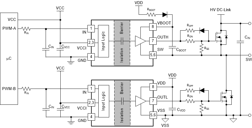
The circuit in Figure 22 shows a reference design with two UCC5304 devices driving a typical half-bridge configuration which could be used in several popular power converter topologies such as synchronous buck, synchronous boost, half-bridge/full bridge isolated topologies, and 3-phase motor drive applications.
 Figure 22. Typical Application Schematic