SLUSDV5B October   2019  – April 2020 UCC5304

PRODUCTION DATA.  

  1. Features
  2. Applications
  3. Description
    1.     Device Images
      1.      Typical Application
  4. Revision History
  5. Pin Configuration and Functions
    1.     Pin Functions
  6. Specifications
    1. 6.1  Absolute Maximum Ratings
    2. 6.2  ESD Ratings
    3. 6.3  Recommended Operating Conditions
    4. 6.4  Thermal Information
    5. 6.5  Power Ratings
    6. 6.6  Insulation Specifications
    7. 6.7  Safety-Related Certifications
    8. 6.8  Safety-Limiting Values
    9. 6.9  Electrical Characteristics
    10. 6.10 Switching Characteristics
    11. 6.11 Typical Characteristics
  7. Parameter Measurement Information
    1. 7.1 Rising and Falling Time
    2. 7.2 Power-up UVLO Delay to OUTPUT
  8. Detailed Description
    1. 8.1 Overview
    2. 8.2 Functional Block Diagram
    3. 8.3 Feature Description
      1. 8.3.1 VDD, VCCI, and Under Voltage Lock Out (UVLO)
      2. 8.3.2 Input Stage
      3. 8.3.3 Output Stage
    4. 8.4 Device Functional Modes
  9. Application and Implementation
    1. 9.1 Application Information
    2. 9.2 Typical Application
      1. 9.2.1 Design Requirements
      2. 9.2.2 Detailed Design Procedure
        1. 9.2.2.1 Designing IN pin Input Filter
        2. 9.2.2.2 Estimating Junction Temperature
        3. 9.2.2.3 Selecting VCCI and VDD Capacitors
          1. 9.2.2.3.1 Selecting a VCCI Capacitor
          2. 9.2.2.3.2 Selecting a VDD Capacitor
  10. 10Power Supply Recommendations
  11. 11Layout
    1. 11.1 Layout Guidelines
      1. 11.1.1 Component Placement Considerations
      2. 11.1.2 Grounding Considerations
      3. 11.1.3 High-Voltage Considerations
      4. 11.1.4 Thermal Considerations
    2. 11.2 Layout Example
  12. 12Mechanical, Packaging, and Orderable Information

Package Options

Mechanical Data (Package|Pins)
Thermal pad, mechanical data (Package|Pins)
Orderable Information

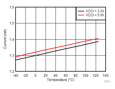
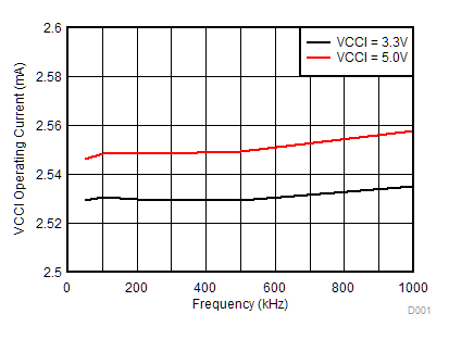
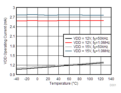
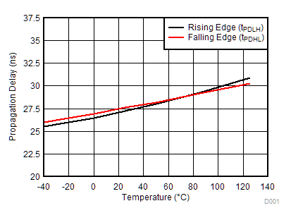
Typical Characteristics

VDD = 12 V, VCCI = 3.3 V or 5.0 V, TA = 25°C, CL=0pF unless otherwise noted.
UCC5304 D003_SLUSCK0.gif
No Load IN = GND
Figure 1. VCCI Quiescent Current
UCC5304 D021_SLUSCK0.gif
Figure 3. VCCI Operating Current vs. Frequency
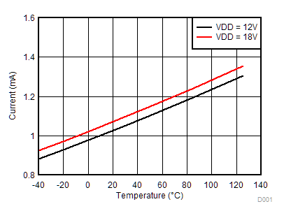
UCC5304 D025_SLUSCK0.gif
No Load
Figure 5. VDD Channel Operating Current (IVDD)
UCC5304 D005_SLUSCK0.gif
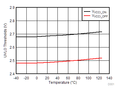
Figure 7. VCCI UVLO Threshold Voltage
UCC5304 UVLO.gif
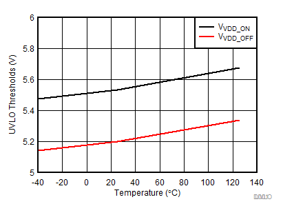
Figure 9. VDD Supply UVLO Threshold Voltage
UCC5304 D012_SLUSCK0.gif
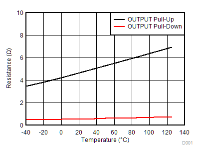
Figure 11. OUT Pullup and Pulldown Resistance
UCC5304 D016_SLUSCK0.gif
tPDLH – tPDHL
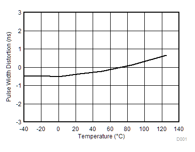
Figure 13. Pulse Width Distortion
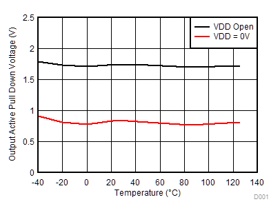
UCC5304 D023_SLUSCK0.gif
Figure 15. OUTPUT Active Pulldown Voltage
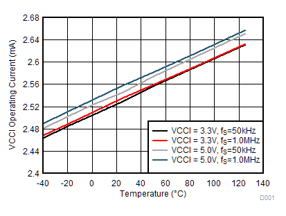
UCC5304 D019_SLUSCK0.gif
Figure 2. VCCI Operating Current - IVCCI
UCC5304 D004_SLUSCK0.gif
No Load IN = GND
Figure 4. VDD Quiescent Current (IVDD)
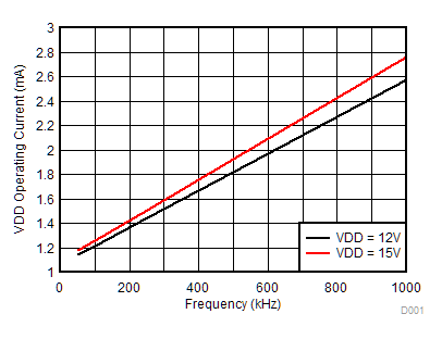
UCC5304 D022_SLUSCK0.gif
No Load IN pin switching
Figure 6. Operating Current (IVDD) vs. Frequency
UCC5304 D006_SLUSCK0.gif
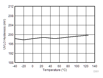
Figure 8. VCCI UVLO Threshold Hysteresis Voltage
UCC5304 UVLOhys.gif
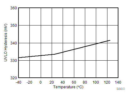
Figure 10. VDD Supply UVLO Threshold Hysteresis
UCC5304 D014_SLUSCK0.gif
Figure 12. Propagation Delay, Rising and Falling Edge
UCC5304 D017_SLUSCK0.gif
CL = 1.8 nF
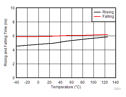
Figure 14. Rise Time and Fall Time
UCC5304 D024_SLUSCK0.gif
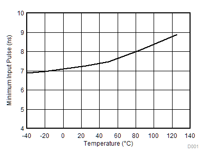
Figure 16. Minimum Pulse that Changes Output