JAJSCA2B June 2016 – January 2018 ADS8910B , ADS8912B , ADS8914B
PRODUCTION DATA.
- 1 特長
- 2 アプリケーション
- 3 概要
- 4 改訂履歴
- 5 Pin Configuration and Functions
- 6 Specifications
-
7 Detailed Description
- 7.1 Overview
- 7.2 Functional Block Diagram
- 7.3 Feature Description
- 7.4 Device Functional Modes
- 7.5
Programming
- 7.5.1 Output Data Word
- 7.5.2 Data Transfer Frame
- 7.5.3 Interleaving Conversion Cycles and Data Transfer Frames
- 7.5.4 Data Transfer Protocols
- 7.5.5 Device Setup
- 7.6
Register Maps
- 7.6.1
Device Configuration and Register Maps
- 7.6.1.1 PD_CNTL Register (address = 04h) [reset = 00h]
- 7.6.1.2 SDI_CNTL Register (address = 008h) [reset = 00h]
- 7.6.1.3 SDO_CNTL Register (address = 0Ch) [reset = 00h]
- 7.6.1.4 DATA_CNTL Register (address = 010h) [reset = 00h]
- 7.6.1.5 PATN_LSB Register (address = 014h) [reset = 00h]
- 7.6.1.6 PATN_MID Register (address = 015h) [reset = 00h]
- 7.6.1.7 PATN_MSB Register (address = 016h) [reset = 00h]
- 7.6.1.8 OFST_CAL Register (address = 020h) [reset = 00h]
- 7.6.1.9 REF_MRG Register (address = 030h) [reset = 00h]
- 7.6.1
Device Configuration and Register Maps
-
8 Application and Implementation
- 8.1 Application Information
- 8.2 Typical Application
- 9 Power-Supply Recommendations
- 10Layout
- 11デバイスおよびドキュメントのサポート
- 12メカニカル、パッケージ、および注文情報
パッケージ・オプション
メカニカル・データ(パッケージ|ピン)
- RGE|24
サーマルパッド・メカニカル・データ
- RGE|24
発注情報
7.5.5.3 Multiple Devices: Daisy-Chain Topology
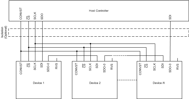
A typical connection diagram showing multiple devices in a daisy-chain topology is shown in Figure 87.
 Figure 87. Daisy-Chain Connections
The CONVST, CS, and SCLK inputs of all devices are connected together and controlled by a single CONVST, CS, and SCLK pin of the host controller, respectively. The SDI input pin of the first device in the chain (Device 1) is connected to the SDO pin of the host controller, the SDO-0 output pin of Device 1 is connected to the SDI input pin of Device 2, and so on. The SDO-0 output pin of the last device in the chain (Device N) is connected to the SDI pin of the host controller.
To operate multiple devices in a daisy-chain topology, the host controller sets the configuration registers in each device with identical values and operates with any of the legacy, SPI-compatible protocols for data-read and data-write operations (SDO_CNT[7:0] = 00h or 01h). With these configurations settings, the 22-bit ODR and 22-bit IDR registers in each device collapse to form a single, 22-bit unified shift register (USR) per device, as shown in Figure 88.
 Figure 88. Unified Shift Register
All devices in the daisy-chain topology sample the respective device analog input signals on the CONVST rising edge. The data transfer frame starts with a CS falling edge. On each SCLK launch edge, every device in the chain shifts out the MSB of the respective USR on to the respective SDO-0 pin. On every SCLK capture edge, each device in the chain shifts in data received on the respective SDI pin as the LSB bit of the respective USR. Therefore, in a daisy-chain configuration, the host controller receives the data of Device N, followed by the data of Device N – 1, and so on (MSB-first). On the CS rising edge, each device decodes the contents in the respective USR, and takes appropriate action.
A typical timing diagram for three devices connected in daisy-chain topology using the SPI-00-S protocol is shown in Figure 89.
 Figure 89. Three-Device, Daisy-Chain Timing
In daisy-chain topology, the overall throughput of the system is proportionally reduced as more devices are connected in the daisy-chain.
NOTE
For N devices connected in daisy-chain topology, an optimal data transfer frame must contain 22 × N SCLK capture edges. For a longer data transfer frame (number of SCLK in the frame > 22 × N), the host controller must appropriately align the configuration data for each device before bringing CS high. A shorter data transfer frame (number of SCLK in the frame < 22 × N) might result in an erroneous device configuration, and must be avoided.