JAJSFX3F august 2012 – april 2023 DLP9500
PRODUCTION DATA
- 1 特長
- 2 アプリケーション
- 3 概要
- 4 Revision History
- 5 Pin Configuration and Functions
-
6 Specifications
- 6.1 Absolute Maximum Ratings
- 6.2 Storage Conditions
- 6.3 ESD Ratings
- 6.4 Recommended Operating Conditions
- 6.5 Thermal Information
- 6.6 Electrical Characteristics
- 6.7 LVDS Timing Requirements
- 6.8 LVDS Waveform Requirements
- 6.9 Serial Control Bus Timing Requirements
- 6.10 Systems Mounting Interface Loads
- 6.11 Micromirror Array Physical Characteristics
- 6.12 Micromirror Array Optical Characteristics
- 6.13 Window Characteristics
- 6.14 Chipset Component Usage Specification
-
7 Detailed Description
- 7.1 Overview
- 7.2 Functional Block Diagram
- 7.3
Feature Description
- 7.3.1 DLPC410 - Digital Controller for DLP Discovery 4100 Chipset
- 7.3.2 DLPA200 - DMD Micromirror Drivers
- 7.3.3 DLPR410 - PROM for DLP Discovery 4100 Chipset
- 7.3.4 DLP9500 - DLP 0.95 1080p 2xLVDS Type-A DMD 1080p DMD
- 7.3.5 Measurement Conditions
- 7.4 Device Functional Modes
- 7.5 Window Characteristics and Optics
- 7.6 Micromirror Array Temperature Calculation
- 7.7 Micromirror Landed-On and Landed-Off Duty Cycle
- 8 Application and Implementation
- 9 Power Supply Recommendations
- 10Layout
- 11Device and Documentation Support
- 12Mechanical, Packaging, and Orderable Information
7.3.4.1.3.2 DLPC410 to DLPA200 IO Description
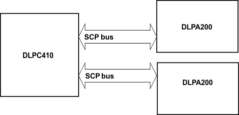
The serial communications port (SCP) is a full duplex, synchronous, character-oriented (byte) port that allows exchange of commands from the DLPC410 to the DLPA200s.
 Figure 7-3 Serial Port System Configuration
Five signal lines are associated with the SCP bus: SCPEN, SCPCK, SCPDI, SCPDO, and IRQ.
Table 7-4 lists the available controls and status pin names and their corresponding signal type, along with a brief functional description.
| PIN NAME | DESCRIPTION | I/O |
|---|---|---|
| A_SCPEN | Active-low chip select for DLPA200 serial bus | O |
| A_STROBE | DLPA200 control signal strobe | O |
| A_MODE(1:0) | DLPA200 mode control | O |
| A_SEL(1:0) | DLPA200 select control | O |
| A_ADDR(3:0) | DLPA200 address control | O |
| B_SCPEN | Active-low chip select for DLPA200 serial bus (2) | O |
| B_STROBE | DLPA200 control signal strobe (2) | O |
| B_MODE(1:0) | DLPA200 mode control | O |
| B_SEL(1:0) | DLPA200 select control | O |
| B_ADDR(3:0) | DLPA200 address control | O |
The DLPA200 provides a variety of output options to the DMD by selecting logic control inputs: MODE[1:0], SEL[1:0] and reset group address A[3:0] (Table 7-4). The MODE[1:0] input determines whether a single output, two outputs, four outputs, or all outputs, will be selected. Output levels (VBIAS, VOFFSET, or VRESET) are selected by SEL[1:0] pins. Selected outputs are tri-stated on the rising edge of the STROBE signal and latched to the selected voltage level after a break-before-make delay. Outputs will remain latched at the last micromirror clocking pulse waveform level until the next micromirror clocking pulse waveform cycle.