JAJSFX3F august 2012 – april 2023 DLP9500
PRODUCTION DATA
- 1 特長
- 2 アプリケーション
- 3 概要
- 4 Revision History
- 5 Pin Configuration and Functions
-
6 Specifications
- 6.1 Absolute Maximum Ratings
- 6.2 Storage Conditions
- 6.3 ESD Ratings
- 6.4 Recommended Operating Conditions
- 6.5 Thermal Information
- 6.6 Electrical Characteristics
- 6.7 LVDS Timing Requirements
- 6.8 LVDS Waveform Requirements
- 6.9 Serial Control Bus Timing Requirements
- 6.10 Systems Mounting Interface Loads
- 6.11 Micromirror Array Physical Characteristics
- 6.12 Micromirror Array Optical Characteristics
- 6.13 Window Characteristics
- 6.14 Chipset Component Usage Specification
-
7 Detailed Description
- 7.1 Overview
- 7.2 Functional Block Diagram
- 7.3
Feature Description
- 7.3.1 DLPC410 - Digital Controller for DLP Discovery 4100 Chipset
- 7.3.2 DLPA200 - DMD Micromirror Drivers
- 7.3.3 DLPR410 - PROM for DLP Discovery 4100 Chipset
- 7.3.4 DLP9500 - DLP 0.95 1080p 2xLVDS Type-A DMD 1080p DMD
- 7.3.5 Measurement Conditions
- 7.4 Device Functional Modes
- 7.5 Window Characteristics and Optics
- 7.6 Micromirror Array Temperature Calculation
- 7.7 Micromirror Landed-On and Landed-Off Duty Cycle
- 8 Application and Implementation
- 9 Power Supply Recommendations
- 10Layout
- 11Device and Documentation Support
- 12Mechanical, Packaging, and Orderable Information
6.4 Recommended Operating Conditions
over operating free-air temperature range (unless otherwise noted)(1)
| MIN | NOM | MAX | UNIT | ||||
|---|---|---|---|---|---|---|---|
| ELECTRICAL (2) (3) | |||||||
| VCC | Supply voltage for LVCMOS core logic | 3.0 | 3.3 | 3.6 | V | ||
| VCC1 | Supply voltage for LVDS receivers | 3.0 | 3.3 | 3.6 | V | ||
| VCC2 | Mirror electrode and HVCMOS supply voltage | 8.25 | 8.5 | 8.75 | V | ||
| VMBRST | Clocking Pulse Waveform Voltage applied to MBRST[29:0] Input Pins (supplied by DLPA200s) | -27 | 26.5 | V | |||
| |VCCI–VCC| | Supply voltage delta (absolute value) (4) | 0.3 | V | ||||
| ENVIRONMENTAL (5) For Illumination Source Between 420 nm and 700 nm | |||||||
| TARRAY | Array temperature, Long–term operational (12)(7) (6)(8) | 20 | 25-45 | 65 (13) | °C | ||
| Array temperature, Short–term operational (12)(7) (9) | 0 | 20 | |||||
| TWINDOW | Window temperature test points TP2 and TP3, Long-term operational(8). | 10 | 70 | °C | |||
| |TDELTA| | Absolute temperature delta between the window test points (TP2, TP3) and the ceramic test point TP1.(11) | 10 | °C | ||||
| ILLVIS | Illumination(10) | Thermally limited | W/cm2 | ||||
| ENVIRONMENTAL (5) For Illumination Source Between 400 nm and 420 nm | |||||||
| TARRAY | Array temperature, Long–term operational (12)(7) (6)(8) | 20 | 30 | °C | |||
| TWINDOW | Window temperature test points TP2 and TP3, Long-term operational(8) | 30 | °C | ||||
| |TDELTA| | Absolute temperature delta between the window test points (TP2, TP3) and the ceramic test point TP1.(11) | 10 | °C | ||||
| ILL | Illumination(10) | 11 | W/cm2 | ||||
| 26.6 | W | ||||||
| ENVIRONMENTAL (5) For Illumination Source <400 nm and >700 nm | |||||||
| TARRAY | Array temperature, Long–term operational (12)(7) (6)(8) | 20 | 40 (13) | °C | |||
| Array temperature, Short–term operational (12)(7) (9) | 0 | 20 | |||||
| TWINDOW | Window temperature test points TP2 and TP3, Long-term operational(8) | 10 | 70 | °C | |||
| ILL | Illumination(10) | 10 | mW/cm2 | ||||
(1) The functional performance of the device specified in this data sheet is achieved when operating the device within the limits defined by the Recommended Operating Conditions. No level of performance is implied when operating the device above or below the Recommended Operating Conditions limits.
(2) Voltages VCC, VCC1, and VCC2 are required for proper DMD operation. VSS must also be connected.
(3) All voltages are referenced to common ground VSS.
(4) Exceeding the recommended allowable absolute voltage difference between VCC and VCC1 may result in excess current draw. The difference between VCC and VCC1, |VCC – VCC1|, should be less than the specified limit.
(5) Optimal, long-term performance and optical efficiency of the Digital Micromirror Device (DMD) can be affected by various application parameters, including illumination spectrum, illumination power density, micromirror landed duty-cycle, ambient temperature (storage and operating), DMD temperature, ambient humidity (storage and operating), and power on or off duty cycle. TI recommends that application-specific effects be considered as early as possible in the design cycle.
(6) Simultaneous exposure of the DMD to the maximum Section 6.4 for temperature and UV illumination will reduce device lifetime.
(7) The array temperature cannot be measured directly and must be computed analytically from the temperature measured at test point 1 (TP1) shown in Figure 7-10 and the package thermal resistance in Section 6.5 using Micromirror Array Temperature Calculation.
(8) Long-term is defined as the usable life of the device.
(9) Array temperatures beyond those specified as long-term are recommended for short-term conditions only (power-up). Short-term is defined as cumulative time over the usable life of the device and is less than 500 hours.
(10) Total integrated illumination power density on the array in the indicated wavelength range.
(11) The temperature delta is the highest difference between the ceramic test point (TP1) and window test points (TP2) and (TP3) in Figure 7-10.
(12) In some applications, the total DMD heat load can be dominated by the amount of incident light energy absorbed. See Micromirror Array Temperature Calculation for further details.
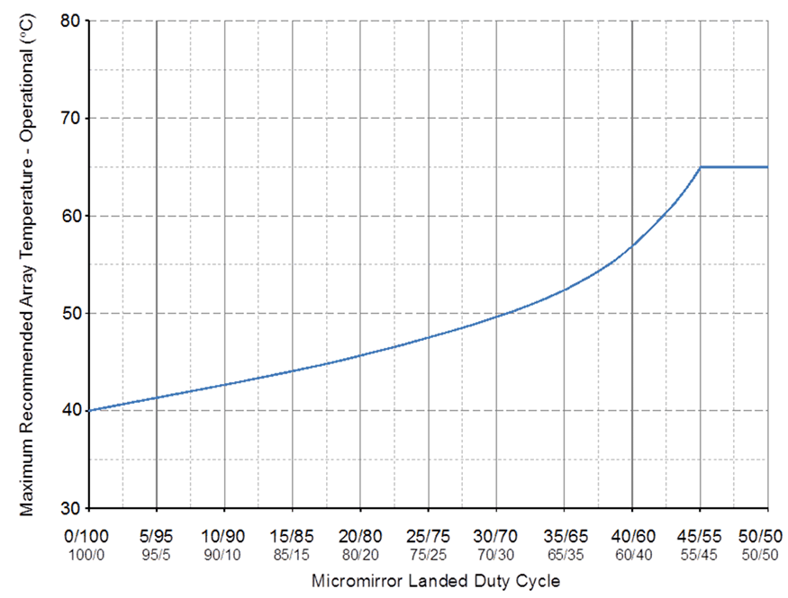
(13) Per Figure 6-1, the maximum operational array temperature should be derated based on the micromirror landed duty cycle that the DMD experiences in the end application. Refer to Section 7.7 for a definition of micromirror landed duty cycle.
 Figure 6-1 Max Recommended DMD Temperature – Derating Curve