JAJSDA0 June 2017 DRV10983-Q1
PRODUCTION DATA.
- 1 特長
- 2 アプリケーション
- 3 概要
- 4 改訂履歴
- 5 Description (Continued)
- 6 Pin Configuration and Functions
- 7 Specifications
-
8 Detailed Description
- 8.1 Overview
- 8.2 Functional Block Diagram
- 8.3 Feature Description
- 8.4
Device Functional Modes
- 8.4.1 Motor Parameters
- 8.4.2 Starting the Motor Under Different Initial Conditions
- 8.4.3 Motor Start Sequence
- 8.4.4 Align Current
- 8.4.5 Start-Up Current Setting
- 8.4.6 Closed Loop
- 8.4.7 Current Limit
- 8.4.8 Lock Detect and Fault Handling
- 8.4.9 Anti Voltage Supression Function
- 8.4.10 PWM Output
- 8.4.11 FG Customized Configuration
- 8.4.12
Diagnostics and Visibility
- 8.4.12.1 Motor-Status Readback
- 8.4.12.2 Motor-Speed Readback
- 8.4.12.3 Motor Electrical-Period Readback
- 8.4.12.4 Motor Velocity Constant Read Back
- 8.4.12.5 Motor Estimated Position by IPD
- 8.4.12.6 Supply-Voltage Readback
- 8.4.12.7 Speed-Command Readback
- 8.4.12.8 Speed-Command Buffer Readback
- 8.4.12.9 Fault Diagnostics
- 8.5
Register Maps
- 8.5.1 I2C Serial Interface
- 8.5.2 Register Map
- 8.5.3
Register Descriptions
- 8.5.3.1 FaultReg Register (address = 0x00) [reset = 0x00]
- 8.5.3.2 MotorSpeed Register (address = 0x01) [reset = 0x00]
- 8.5.3.3 MotorPeriod Register (address = 0x02) [reset = 0x00]
- 8.5.3.4 MotorKt Register (address = 0x03) [reset = 0x00]
- 8.5.3.5 MotorCurrent Register (address = 0x04) [reset = 0x00]
- 8.5.3.6 IPDPosition-SupplyVoltage Register (address = 0x05) [reset = 0x00]
- 8.5.3.7 SpeedCmd-spdCmdBuffer Register (address = 0x06) [reset = 0x00]
- 8.5.3.8 AnalogInLvl Register (address = 0x07) [reset = 0x00]
- 8.5.3.9 DeviceID-RevisionID Register (address = 0x08) [reset = 0x00]
- 8.5.3.10 DeviceID-RevisionID Register (address = 0x08) [reset = 0x00]
- 8.5.3.11 Unused Registers (addresses = 0x011 Through 0x2F)
- 8.5.3.12 SpeedCtrl Register (address = 0x30) [reset = 0x00]
- 8.5.3.13 EEPROM Programming1 Register (address = 0x31) [reset = 0x00]
- 8.5.3.14 EEPROM Programming2 Register (address = 0x32) [reset = 0x00]
- 8.5.3.15 EEPROM Programming3 Register (address = 0x33) [reset = 0x00]
- 8.5.3.16 EEPROM Programming4 Register (address = 0x34) [reset = 0x00]
- 8.5.3.17 EEPROM Programming5 Register (address = 0xYY) [reset = 0x00]
- 8.5.3.18 EEPROM Programming6 Register (address = 0x36) [reset = 0x00]
- 8.5.3.19 Unused Registers (addresses = 0x37 Through 0x5F)
- 8.5.3.20 EECTRL Register (address = 0x60) [reset = 0x00]
- 8.5.3.21 Unused Registers (addresses = 0x61 Through 0x8F)
- 8.5.3.22 CONFIG1 Register (address = 0x90) [reset = 0x00]
- 8.5.3.23 CONFIG2 Register (address = 0x91) [reset = 0x00]
- 8.5.3.24 CONFIG3 Register (address = 0x92) [reset = 0x00]
- 8.5.3.25 CONFIG4 Register (address = 0x93) [reset = 0x00]
- 8.5.3.26 CONFIG5 Register (address = 0x94) [reset = 0x00]
- 8.5.3.27 CONFIG6 Register (address = 0x95) [reset = 0x00]
- 8.5.3.28 CONFIG7 Register (address = 0x96) [reset = 0x00]
- 9 Application and Implementation
- 10Power Supply Recommendations
- 11Layout
- 12デバイスおよびドキュメントのサポート
- 13メカニカル、パッケージ、および注文情報
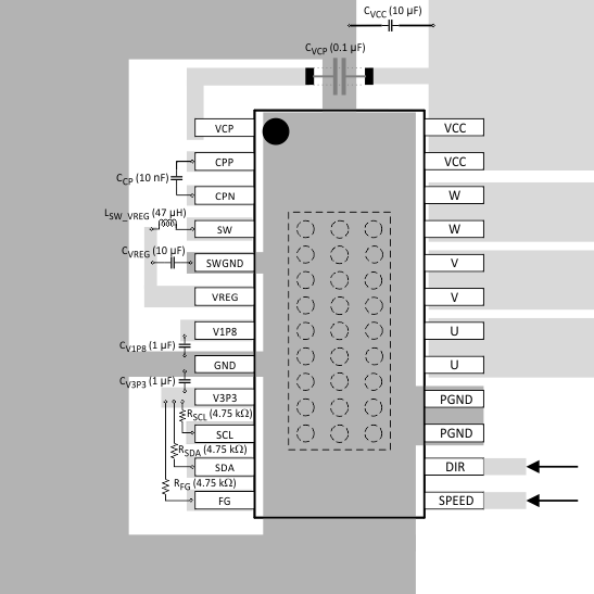
11 Layout
11.1 Layout Guidelines
- Place the VCC, GND, U, V, and W pins with thick traces because high current passes through these traces.
- Place the 10-µF capacitor between VCC and GND, and as close to the VCC and GND pins as possible.
- Place the capacitor between CPP and CPN, and as close to the CPP and CPN pins as possible.
- Connect the GND, PGND, and SWGND under the thermal pad.
- Keep the thermal pad connection as large as possible, on both the bottom side and top sides. It should be one piece of copper without any gaps.
11.2 Layout Example
 Figure 70. Layout Diagram