JAJSDA0 June 2017 DRV10983-Q1
PRODUCTION DATA.
- 1 特長
- 2 アプリケーション
- 3 概要
- 4 改訂履歴
- 5 Description (Continued)
- 6 Pin Configuration and Functions
- 7 Specifications
-
8 Detailed Description
- 8.1 Overview
- 8.2 Functional Block Diagram
- 8.3 Feature Description
- 8.4
Device Functional Modes
- 8.4.1 Motor Parameters
- 8.4.2 Starting the Motor Under Different Initial Conditions
- 8.4.3 Motor Start Sequence
- 8.4.4 Align Current
- 8.4.5 Start-Up Current Setting
- 8.4.6 Closed Loop
- 8.4.7 Current Limit
- 8.4.8 Lock Detect and Fault Handling
- 8.4.9 Anti Voltage Supression Function
- 8.4.10 PWM Output
- 8.4.11 FG Customized Configuration
- 8.4.12
Diagnostics and Visibility
- 8.4.12.1 Motor-Status Readback
- 8.4.12.2 Motor-Speed Readback
- 8.4.12.3 Motor Electrical-Period Readback
- 8.4.12.4 Motor Velocity Constant Read Back
- 8.4.12.5 Motor Estimated Position by IPD
- 8.4.12.6 Supply-Voltage Readback
- 8.4.12.7 Speed-Command Readback
- 8.4.12.8 Speed-Command Buffer Readback
- 8.4.12.9 Fault Diagnostics
- 8.5
Register Maps
- 8.5.1 I2C Serial Interface
- 8.5.2 Register Map
- 8.5.3
Register Descriptions
- 8.5.3.1 FaultReg Register (address = 0x00) [reset = 0x00]
- 8.5.3.2 MotorSpeed Register (address = 0x01) [reset = 0x00]
- 8.5.3.3 MotorPeriod Register (address = 0x02) [reset = 0x00]
- 8.5.3.4 MotorKt Register (address = 0x03) [reset = 0x00]
- 8.5.3.5 MotorCurrent Register (address = 0x04) [reset = 0x00]
- 8.5.3.6 IPDPosition-SupplyVoltage Register (address = 0x05) [reset = 0x00]
- 8.5.3.7 SpeedCmd-spdCmdBuffer Register (address = 0x06) [reset = 0x00]
- 8.5.3.8 AnalogInLvl Register (address = 0x07) [reset = 0x00]
- 8.5.3.9 DeviceID-RevisionID Register (address = 0x08) [reset = 0x00]
- 8.5.3.10 DeviceID-RevisionID Register (address = 0x08) [reset = 0x00]
- 8.5.3.11 Unused Registers (addresses = 0x011 Through 0x2F)
- 8.5.3.12 SpeedCtrl Register (address = 0x30) [reset = 0x00]
- 8.5.3.13 EEPROM Programming1 Register (address = 0x31) [reset = 0x00]
- 8.5.3.14 EEPROM Programming2 Register (address = 0x32) [reset = 0x00]
- 8.5.3.15 EEPROM Programming3 Register (address = 0x33) [reset = 0x00]
- 8.5.3.16 EEPROM Programming4 Register (address = 0x34) [reset = 0x00]
- 8.5.3.17 EEPROM Programming5 Register (address = 0xYY) [reset = 0x00]
- 8.5.3.18 EEPROM Programming6 Register (address = 0x36) [reset = 0x00]
- 8.5.3.19 Unused Registers (addresses = 0x37 Through 0x5F)
- 8.5.3.20 EECTRL Register (address = 0x60) [reset = 0x00]
- 8.5.3.21 Unused Registers (addresses = 0x61 Through 0x8F)
- 8.5.3.22 CONFIG1 Register (address = 0x90) [reset = 0x00]
- 8.5.3.23 CONFIG2 Register (address = 0x91) [reset = 0x00]
- 8.5.3.24 CONFIG3 Register (address = 0x92) [reset = 0x00]
- 8.5.3.25 CONFIG4 Register (address = 0x93) [reset = 0x00]
- 8.5.3.26 CONFIG5 Register (address = 0x94) [reset = 0x00]
- 8.5.3.27 CONFIG6 Register (address = 0x95) [reset = 0x00]
- 8.5.3.28 CONFIG7 Register (address = 0x96) [reset = 0x00]
- 9 Application and Implementation
- 10Power Supply Recommendations
- 11Layout
- 12デバイスおよびドキュメントのサポート
- 13メカニカル、パッケージ、および注文情報
8 Detailed Description
8.1 Overview
The DRV10983-Q1 device is a three-phase sensorless motor driver with integrated power MOSFETs that provides drive-current capability up to 2 A continuously. The device is specifically designed for low-noise, low-external-component-count motor-drive applications. The device is configurable through a simple I2C interface to accommodate different motor parameters and spin-up profiles for different customer applications.
A 180° sensorless control scheme provides continuous sinusoidal output voltages to the motor phases to enable ultra-quiet motor operation by keeping the electrically induced torque ripple small.
The DRV10983-Q1 device features extensive protection and fault-detection mechanisms to ensure reliable operation. Voltage surge protection prevents the input VCC capacitor from overcharging, which is typical during motor deceleration. The device provides overcurrent protection without the need for an external current-sense resistor. Rotor-lock detection is available through several methods. These methods can be configured with register settings to ensure reliable operation. The device provides additional protection for undervoltage lockout (UVLO) and for thermal shutdown.
The commutation control algorithm continuously measures the motor phase current and periodically measures the VCC supply voltage. The device uses this information for BEMF estimation, and the information is also provided through the I2C register interface for debug and diagnostic use in the system, if desired.
A buck switching regulator efficiently steps down the supply voltage. The output of this regulator provides power for the internal circuits and can also be used to provide power for an external circuit such as a microcontroller. If providing power for an external circuit is not necessary (and to reduce system cost), configure the buck switching regulator as a linear regulator by replacing the inductor with a resistor.
The DRV10983-Q1 device has a flexible interface, capable of supporting both analog and digital inputs. In addition to the I2C interface, the device has FG, DIR, and SPEED pins. SPEED is the speed command input pin. DIR is the direction control input pin. FG is the speed indicator output, which shows the frequency of the motor commutation.
EEPROM is integrated in the DRV10983-Q1 device as memory for the motor parameter and operation settings. EEPROM data transfers to the registers after power-on and exit from sleep mode.
The DRV10983-Q1 device can also operate in register mode. If the system includes a microcontroller communicating through the I2C interface, the device can dynamically update the motor parameters and operation settings by writing to the registers. In this configuration, the EEPROM data is bypassed by the register settings.
8.2 Functional Block Diagram
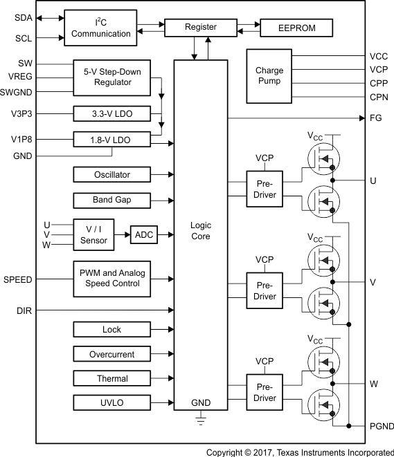
8.3 Feature Description
8.3.1 Regulators
8.3.1.1 Step-Down Regulator
The DRV10983-Q1 device includes a step-down hysteretic voltage regulator that can operate with either an external inductor or with an external resistor. The best efficiency is achieved when an external inductor (see Figure 3) is used. The regulator output voltage is 5 V. When the regulated voltage drops by the hysteresis level, the high-side FET turns on to raise the regulated voltage back to the target of 5 V. The switching frequency of the hysteretic regulator is not constant and changes with load.
If the step-down regulator is configured with an external inductor, it can deliver current to the load as specified by IREG_MAX_L. If the step-down regulator is configured with an external resistor it, can deliver current to the load as specified by IREG_MAX_R.

| Buck Regulator with External Inductor | Buck Regulator with External Resistor |
8.3.1.2 3.3-V and 1.8-V LDO
The DRV10983-Q1 device includes a 3.3-V LDO and a 1.8-V LDO. The 1.8-V LDO is for internal circuits only. The 3.3-V LDO is mainly for internal circuits, but can also drive external loads not to exceed IV3P3_MAX. For example, it can work as a pullup voltage for the FG, DIR, SDA, and SCL interface.
Both the V1P8 and V3P3 capacitors must be connected to GND.
8.3.2 Protection Circuits
8.3.2.1 Thermal Shutdown
The DRV10983-Q1 device has a built-in thermal shutdown function, which shuts down the device when the junction temperature is more than TSDN˚C and recovers operating conditions when the junction temperature falls to TSDN – TSDN_HYS˚C.
The OverTemp status bit (address 0x00, bit 15) is set during thermal shutdown. In addition to the thermal shutdown function there is a warning bit that is set whenever the device exceeds TWARN and is indicated by the TempWarning bit of the FaultReg register (address 0x00, bit 14).
8.3.2.2 UVLO
The DRV10983-Q1 device has a built-in UVLO function block. The device is locked out when VCC is below VUVLO_F and is unlocked when VCC is above VUVLO_R. The hysteresis of the UVLO threshold is VUVLO_HYS. In addition to the main supply, the step-down regulator, charge pump, and 3.3-V LDO all have undervoltage lockout monitors.
8.3.2.3 Current Protection
The overcurrent shutdown function acts to protect the device if the current, as measured from the FETs, exceeds the IOC-limit threshold. It protects the device in the event of a short-circuit condition on the motor phases. This includes phase shorts to GND, phase shorts to phase, or phase shorts to VCC. The DRV10983-Q1 device places the output drivers into a high-impedance state until the lock time tLOCK_OFF has expired. The OverCurr status bit of the FaultReg register (address 0x00, bit 11) is set.
The DRV10983-Q1 device also provides acceleration current-limit and lock-detection current-limit functions to protect the device and motor (see Current Limit and Lock Detect and Fault Handling ).
8.3.2.4 Lock
When the motor is blocked or stopped by an external force, lock protection is triggered, and the device stops driving the motor immediately. After the lock release time tLOCK_OFF, the DRV10983-Q1 device resumes driving the motor again. If the lock condition is still present, it enters the next lock protection cycle, and repeats until the lock condition is removed. With this lock protection, the motor and device do not overheat or become damaged due to the motor being locked (see Lock Detect and Fault Handling ).
During a lock condition the Status register indicates which of the locks has occurred.
8.3.3 Motor Speed Control
The DRV10983-Q1 device offers four methods for indirectly controlling the speed of the motor by adjusting the output voltage amplitude. This can be accomplished by varying the supply voltage (VCC) or by controlling the speed command. The speed command can be controlled in one of three ways. The user can set the speed command by adjusting either the PWM input (PWM in) or the analog input (Analog) or by writing the speed command directly through the I2C serial port (I2C). The speed command is used to determine the PWM duty cycle output (PWM_DCO) (see Figure 5).
The input PWM input (PWM in) can have a minimum duty cycle limit applied. DutyCycleLimit[1:0], accessible through the I2C interface, allows the user to configure the minimum duty cycle behavior. This behavior is illustrated in Figure 4.
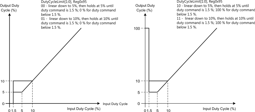 Figure 4. Duty Cycle Profile
The speed command may not always be equal to the PWM_DCO because the DRV10983-Q1 device has the AVS function (see Anti Voltage Supression Function), the acceleration current-limit function (see Acceleration Current Limit), and the closed-loop accelerate function (see Closed-Loop Accelerate) to optimize the control performance. These functions can limit the PWM_DCO, which affects the output amplitude (see Figure 5).
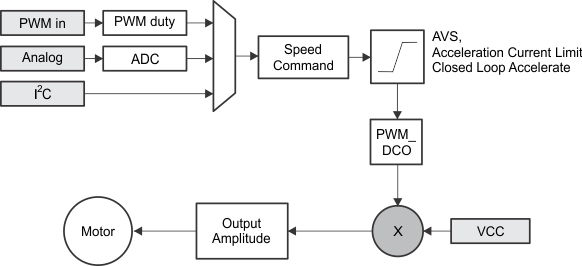 Figure 5. Multiplexing the Speed Command to the Output Amplitude Applied to the Motor
The output voltage amplitude applied to the motor is developed through sine wave modulation so that the phase-to-phase voltage is sinusoidal.
When any phase is measured with respect to ground, the waveform is sinusoidally coupled with third-order harmonics. This encoding technique permits one phase to be held at ground while the other two phases are pulse-width modulated. Figure 6 and Figure 7 show the sinusoidal encoding technique used in the DRV10983-Q1 device.
 Figure 6. PWM Output and the Average Value

| Sinusoidal voltage from phase to phase | Sinusoidal voltage with third-order harmonics from phase to GND |
The output amplitude is determined by the magnitude of VCC and the PWM duty cycle output (PWM_DCO). The PWM_DCO represents the peak duty cycle that is applied in one electrical cycle. The maximum amplitude is reached when PWM_DCO is at 100%. The peak output amplitude is VCC. When the PWM_DCO is at 50%, the peak amplitude is VCC / 2 (see Figure 8).
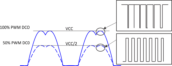 Figure 8. Output Voltage Amplitude Adjustment
Motor speed is controlled indirectly by controlling the output amplitude, which is achieved by either controlling VCC, or controlling the PWM_DCO. The DRV10983-Q1 device provides different options for the user to control the PWM_DCO:
- Analog input (SPEED pin)
- PWM encoded digital input (SPEED pin)
- I2C serial interface.
See the Closed Loop section for more information.
8.3.4 Load Dump Handling
The recommended operation voltage of the DRV10983-Q1 device is from 6.2 V to 28 V. The device is able to drive the motor within this VCC range.
In the load dump condition, VCC can rise up to 45 V. Once the DRV10983-Q1 device detects that VCC is higher than VOV_R3 , it stops driving the motor and protects its own circuitry. When VCC drops below VOV_F, the DRV10983-Q1 device continues to operate the motor based on the user’s command.
8.3.5 Sleep or Standby Condition
The DRV10983-Q1 device is available in either a sleep mode (DRV10983Q) or standby mode version (DRV10983SQ). The DRV10983-Q1 device enters either sleep or standby to conserve energy. When the device enters either sleep or standby, the device stops driving the motor. The switching regulator is disabled in the sleep mode version to conserve more energy. The I2C interface is disabled and any register data not stored in EEPROM is reset for the sleep mode version. The switching regulator remains active in the standby mode version. The register data is maintained, and the I2C interface remains active for standby mode version.
For different speed command modes, Table 1 shows the timing and command to enter the sleep or standby condition.
Table 1. Conditions to Enter or Exit Sleep or Standby Condition
| SPEED COMMAND MODE | ENTER SLEEP OR STANDBY CONDITION | EXIT FROM STANDBY CONDITION | EXIT FROM SLEEP CONDITION |
|---|---|---|---|
| Analog | SPEED pin voltage < VEN_SL_SB for tEN_SL_SB | SPEED pin voltage > VEX_SB for tEX_ SB | SPEED pin high (V > VDIG_IH) for tEX_SL_SB |
| PWM | SPEED pin low (V < VDIG_IL) for tEN_SL_SB | SPEED pin high (V > VDIG_IH) for tEX_SL_SB | SPEED pin high (V > VDIG_IH) for tEX_SL_SB (1) |
| I2C | SpdCtrl[8:0] is programmed as 0 for tEN_SL_SB | SpdCtrl[8:0] is programmed as non-zero for tEX_SL_SB | SPEED pin high (V > VDIG_IH) for tEX_SL_SB |
Note that when using the analog speed command, a higher voltage is required to exit from the sleep condition than from the standby condition. The I2C speed command cannot take the device out of the sleep condition because I2C communication is disabled during the sleep condition.
Table 2. Minimum PWM Duty Cycle Requirement for Different PWM Frequency to Exit Sleep Condition
| INPUT PWM FREQUENCY (kHz) | PWM DUTY CYCLE (%) |
|---|---|
| 0.1 to 0.5 | 14 |
| 0.5 to 1 | 11 |
| 1 to 50 | 9 |
| 50 to 100 | 4 |
| 100 | 3.5 |
8.3.6 EEPROM Access
The DRV10983-Q1 device has 112 bits (7 registers with 16-bit width) of EEPROM data, which are used to program the motor parameters as described in the I2C Serial Interface.
The procedure for programming the EEPROM is as follows. TI recommends to perform the EEPROM programming without the motor spinning, cycle the power after the EEPROM write, and read back the EEPROM to verify the programming is successful.
- Power up with any voltage within operating voltage range (6.2 V to 28 V)
- (DRV10983Q only) Exit from sleep condition
- Wait 10 ms
- Write register 0x60 to set MTR_DIS = 1; this disables the motor driver.
- Write register 0x31 with 0x0000 to clear the EEPROM access code
- Write register 0x31 with 0xC0DE to enable access to EEPROM
- Read register 0x32 for eeReadyStatus = 1
- Case-A: Mass Write
- Write all individual shadow registers
- Write register 0x90 (CONFIG1) with CONFIG1 data
- ...
- Write register 0x96 (CONFIG7) with CONFIG7 data
- Write the following to register 0x35
- ShadowRegEn = 0
- eeRefresh = 0
- eeWRnEn = 1
- EEPROM Access Mode = 10
- Wait for register 0x32 eeReadyStatus = 1 – EEPROM is now updated with the contents of the shadow registers.
- Write all individual shadow registers
- Case-B: Mass Read
- Write the following to register 0x35
- ShadowRegEn = 0
- eeRefresh = 0
- eeWRnEn = 0
- eeAccMode = 10
- Internally, the device starts reading the EEPROM and storing it in the shadow registers.
- Wait for register 0x32 eeReadyStatus = 1 – shadow registers now contain the EEPROM values
- Write the following to register 0x35
- Write register 0x60 to set MTR_DIS = 0; this re-enables the motor driver
8.4 Device Functional Modes
This section includes the logic required to be able to reliably start and drive the motor. It describes the processes used in the logic core and provides the information needed to configure the parameters effectively to work over a wide range of applications.
8.4.1 Motor Parameters
See the DRV10983-Q1 Tuning Guide for the motor parameter measurement.
The motor resistance and motor velocity constants are two important parameters used to characterize a BLDC motor. The DRV10983-Q1 device requires these parameters to be configured in the register. The motor resistance is programmed by writing the values for Rm[6:0] (combination of RMShift[2:0] and RMValue[3:0]) in the Config1 register. The motor velocity constant is programmed by writing the values for Kt[6:0] (combination of KTShift[2:0] and KTValue[3:0]) in the Config2 register.
8.4.1.1 Motor Resistance
For a wye-connected motor, the motor phase resistance refers to the resistance from the phase output to the center tap, RPH_CT (denoted as RPH_CT in Figure 9).
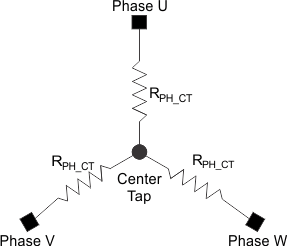 Figure 9. Wye-Connected Motor Resistance
For a delta-connected motor, the motor phase resistance refers to the equivalent phase to center tap in the wye configuration. In Figure 10, it is denoted as RY. RPH_CT = RY.
For both the delta-connected motor and the wye-connected motor, the easy way to get the equivalent RPH_CT is to measure the resistance between two phase terminals (RPH_PH), and then divide this value by two, RPH_CT = ½ RPH_PH.
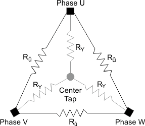 Figure 10. Delta-Connected Motor and the Equivalent Wye Connections
The motor resistance (RPH_CT) must be converted to a 7-bit digital register value Rm[6:0] to program the motor resistance value. The digital register value can be determined as follows:
- Convert the motor resistance (RPH_CT) to a digital value where the LSB is weighted to represent 9.67 mΩ: Rmdig = RPH_CT / 0.00967.
- Encode the digital value such that Rmdig = RMValue[3:0] << RMShift[2:0].
The maximum resistor value, RPH_CT, that can be programmed for the DRV10983-Q1 device is 18.5 Ω, which represents Rmdig = 1920 and an encoded Rm[6:0] value of 0x7Fh. The minimum resistor the DRV10983-Q1 device supports is 0.029 Ω, RPH_CT, which represents Rmdig = 3.
For convenience, the encoded value for Rm[6:0] can also be obtained from Table 3.
Table 3. Motor Resistance Look-Up Table
| RM[6:0] {RMShift[2:0], RMValue[3:0]} | RPH_CT (Ω) | RM[6:0] {RMShift[2:0], RMValue[3:0]} | RPH_CT (Ω) | RM[6:0] {RMShift[2:0], RMValue[3:0]} | RPH_CT (Ω) | |||
|---|---|---|---|---|---|---|---|---|
| BINARY | HEX | BINARY | HEX | BINARY | HEX | |||
| 000 0000 | 0x00 | 0 | 0101000 | 0x28 | 0.3104 | 1011000 | 0x58 | 2.4832 |
| 000 0001 | 0x01 | 0.0097 | 010 1001 | 0x29 | 0.3492 | 101 1001 | 0x59 | 2.7936 |
| 000 0010 | 0x02 | 0.0194 | 010 1010 | 0x2A | 0.388 | 101 1010 | 0x5A | 3.104 |
| 000 0011 | 0x03 | 0.0291 | 010 1011 | 0x2B | 0.4268 | 101 1011 | 0x5B | 3.4144 |
| 000 0100 | 0x04 | 0.0388 | 010 1100 | 0x2C | 0.4656 | 101 1100 | 0x5C | 3.7248 |
| 000 0101 | 0x05 | 0.0485 | 010 1101 | 0x2D | 0.5044 | 101 1101 | 0x5D | 4.0352 |
| 000 0110 | 0x06 | 0.0582 | 010 1110 | 0x2E | 0.5432 | 101 1110 | 0x5E | 4.3456 |
| 000 0111 | 0x07 | 0.0679 | 010 1111 | 0x2F | 0.582 | 101 1111 | 0x5F | 4.656 |
| 000 1000 | 0x08 | 0.0776 | 011 1000 | 0x38 | 0.6208 | 110 1000 | 0x68 | 4.9664 |
| 000 1001 | 0x09 | 0.0873 | 011 1001 | 0x39 | 0.6984 | 110 1001 | 0x69 | 5.5872 |
| 000 1010 | 0x0A | 0.097 | 011 1010 | 0x3A | 0.776 | 110 1010 | 0x6A | 6.208 |
| 000 1011 | 0x0B | 0.1067 | 011 1011 | 0x3B | 0.8536 | 110 1011 | 0x6B | 6.8288 |
| 000 1100 | 0x0C | 0.1164 | 011 1100 | 0x3C | 0.9312 | 110 1100 | 0x6C | 7.4496 |
| 000 1101 | 0x0D | 0.1261 | 011 1101 | 0x3D | 1.0088 | 110 1101 | 0x6D | 8.0704 |
| 000 1110 | 0x0E | 0.1358 | 011 1110 | 0x3E | 1.0864 | 110 1110 | 0x6E | 8.6912 |
| 000 1111 | 0x0F | 0.1455 | 011 1111 | 0x3F | 1.164 | 110 1111 | 0x6F | 9.312 |
| 001 1000 | 0x18 | 0.1552 | 100 1000 | 0x48 | 1.2416 | 111 1000 | 0x78 | 9.9328 |
| 001 1001 | 0x19 | 0.1746 | 100 1001 | 0x49 | 1.3968 | 111 1001 | 0x79 | 11.1744 |
| 001 1010 | 0x1A | 0.194 | 100 1010 | 0x4A | 1.552 | 111 1010 | 0x7A | 12.416 |
| 001 1011 | 0x1B | 0.2134 | 100 1011 | 0x4B | 1.7072 | 111 1011 | 0x7B | 13.6576 |
| 001 1100 | 0x1C | 0.2328 | 100 1100 | 0x4C | 1.8624 | 111 1100 | 0x7C | 14.8992 |
| 001 1101 | 0x1D | 0.2522 | 100 1101 | 0x4D | 2.0176 | 111 1101 | 0x7D | 16.1408 |
| 001 1110 | 0x1E | 0.2716 | 100 1110 | 0x4E | 2.1728 | 111 1110 | 0x7E | 17.3824 |
| 001 1111 | 0x1F | 0.291 | 100 1111 | 0x4F | 2.328 | 111 1111 | 0x7F | 18.624 |
8.4.1.2 Motor Velocity Constant
The motor velocity constant, Kt[6:0] describes the phase-to-phase BEMF voltage of the motor as a function of the motor velocity.
Figure 11 shows the measurement technique for this constant as used in the DRV10983-Q1 device.
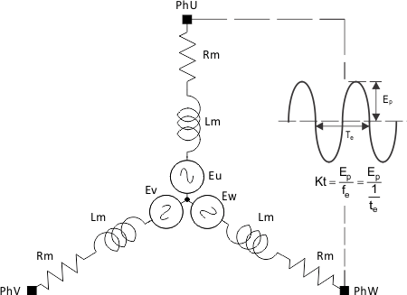 Figure 11. KtPH Definition
With the motor coasting, use an oscilloscope to capture the differential voltage waveform between any two phases. Derive the motor velocity constant used by the DRV10983-Q1 device as shown in Equation 1.
where
- Ep is ½ the peak-to-peak amplitude of the measured voltage
- te is the electrical period
The measured motor velocity constant (KtPH) must be converted to a 7-bit digital register value Kt[6:0] (combination of KtShift[2:0] and KtValue[3:0]) to program the motor velocity constant value. The digital register value can be determined as follows:
- Convert the measured KtPH to a weighted digital value: Ktph_dig = 1090 × KtPH
- Encode the digital value such that Ktph_dig = KtValue[3:0] << KtShift[2:0].
The maximum KtPH that can be programmed is 1760 mV/Hz. This represents a digital value of 1920 and an encoded Kt[6:0] value of 0x7Fh. The minimum KtPH that can be programmed is 0.92 mV/Hz, which represents a digital value of 1 and an encoded Kt[6:0] value of 0x01h.
For convenience, the encoded value of Kt[6:0] may also be obtained from Table 4.
Table 4. Motor Velocity Constant Look-Up Table
| Kt[6:0] {KtShift[2:0], KtValue[3:0]} | KtPH (mV/Hz) | Kt [6:0] {KtShift[2:0], KtValue[3:0]} | KtPH (mV/Hz) | Kt [6:0] {KtShift[2:0], KtValue[3:0]} | KtPH (mV/Hz) | |||
|---|---|---|---|---|---|---|---|---|
| BINARY | HEX | BINARY | HEX | BINARY | HEX | |||
| 000 0000 | 0x00 | 0 | 010 1000 | 0x28 | 29.44 | 101 1000 | 0x58 | 235.52 |
| 000 0001 | 0x01 | 0.92 | 010 1000 | 0x29 | 33.12 | 101 1000 | 0x59 | 264.96 |
| 000 0010 | 0x02 | 1.84 | 010 1000 | 0x2A | 36.8 | 101 1000 | 0x5A | 294.4 |
| 000 0011 | 0x03 | 2.76 | 010 1000 | 0x2B | 40.48 | 101 1000 | 0x5B | 323.84 |
| 000 0100 | 0x04 | 3.68 | 010 1000 | 0x2C | 44.16 | 101 1000 | 0x5C | 353.28 |
| 000 0101 | 0x05 | 4.6 | 010 1000 | 0x2D | 47.84 | 101 1000 | 0x5D | 382.72 |
| 000 0110 | 0x06 | 5.52 | 010 1000 | 0x2E | 51.52 | 101 1000 | 0x5E | 412.16 |
| 000 0111 | 0x07 | 6.44 | 010 1000 | 0x2F | 55.2 | 101 1000 | 0x5F | 441.6 |
| 000 1000 | 0x08 | 7.36 | 011 1000 | 0x38 | 58.88 | 110 1000 | 0x68 | 471.04 |
| 000 1001 | 0x09 | 8.28 | 011 1000 | 0x39 | 66.24 | 110 1000 | 0x69 | 529.92 |
| 000 1010 | 0x0A | 9.2 | 011 1000 | 0x3A | 73.6 | 110 1000 | 0x6A | 588.8 |
| 000 1011 | 0x0B | 10.12 | 011 1000 | 0x3B | 80.96 | 110 1000 | 0x6B | 647.68 |
| 000 1100 | 0x0C | 11.04 | 011 1000 | 0x3C | 88.32 | 110 1000 | 0x6C | 706.56 |
| 000 1101 | 0x0D | 11.96 | 011 1000 | 0x3D | 95.68 | 110 1000 | 0x6D | 765.44 |
| 000 1110 | 0x0E | 12.88 | 011 1000 | 0x3E | 103.04 | 110 1000 | 0x6E | 824.32 |
| 000 1111 | 0x0F | 13.8 | 011 1000 | 0x3F | 110.4 | 110 1000 | 0x6F | 883.2 |
| 001 1000 | 0x18 | 14.72 | 100 1000 | 0x48 | 117.76 | 111 1000 | 0x78 | 942.08 |
| 001 1001 | 0x19 | 16.56 | 100 1000 | 0x49 | 132.48 | 111 1000 | 0x79 | 1059.84 |
| 001 1010 | 0x1A | 18.4 | 100 1000 | 0x4A | 147.2 | 111 1000 | 0x7A | 1177.6 |
| 001 1011 | 0x1B | 20.24 | 100 1000 | 0x4B | 161.92 | 111 1000 | 0x7B | 1295.36 |
| 001 1100 | 0x1C | 22.08 | 100 1000 | 0x4C | 176.64 | 111 1000 | 0x7C | 1413.12 |
| 001 1101 | 0x1D | 23.92 | 100 1000 | 0x4D | 191.36 | 111 1000 | 0x7D | 1530.88 |
| 001 1110 | 0x1E | 25.76 | 100 1000 | 0x4E | 206.08 | 111 1000 | 0x7E | 1648.64 |
| 001 1111 | 0x1F | 27.6 | 100 1000 | 0x4F | 220.8 | 111 1000 | 0x7F | 1766.4 |
8.4.2 Starting the Motor Under Different Initial Conditions
The motor can be in one of three states when the DRV10983-Q1 device attempts to begin the start-up process. The motor may be stationary, or spinning in the forward or reverse directions. The DRV10983-Q1 device includes a number of features to allow for reliable motor start under all of these conditions. Figure 12 shows the motor start-up flow for each of the three initial motor states.
8.4.2.1 Case 1 – Motor is Stationary
If the motor is stationary, the commutation logic must be initialized to be in phase with the position of the motor. The DRV10983-Q1 device provides for two options to initialize the commutation logic to the motor position. Initial position detect (IPD) determines the position of the motor based on the deterministic inductance variation, which is often present in BLDC motors. The align-and-go technique forces the motor into alignment by applying a voltage across a particular motor phase to force the motor to rotate in alignment with this phase.
8.4.2.2 Case 2 – Motor is Spinning in the Forward Direction
If the motor is spinning forward with enough velocity, the DRV10983-Q1 device may be configured to go directly into closed loop. By resynchronizing to the spinning motor, the user achieves the fastest possible start-up time for this initial condition.
8.4.2.3 Case 3 – Motor is Spinning in the Reverse Direction
If the motor is spinning in the reverse direction, the DRV10983-Q1 device provides several methods to convert it back to the forward direction.
One method, reverse drive, allows the motor to be driven so that it accelerates through zero velocity. The motor achieves the shortest possible spin-up time in systems where the motor is spinning in the reverse direction.
If this feature is not selected, then the DRV10983-Q1 device may be configured either to wait for the motor to stop spinning or to brake the motor. After the motor has stopped spinning, the motor start-up sequence proceeds as it would for a motor which is stationary.
Take care when using the reverse-drive or brake feature to ensure that the current is limited to an acceptable level and that the supply voltage does not surge as a result of energy being returned to the power supply.
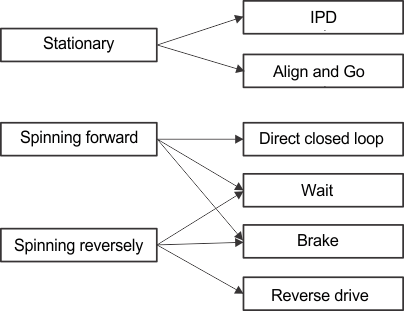 Figure 12. Start the Motor Under Different Initial Conditions
8.4.3 Motor Start Sequence
Figure 13 shows the motor-start sequence implemented in the DRV10983-Q1 device.
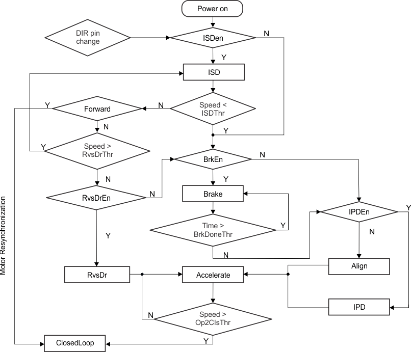 Figure 13. Motor Starting-Up Flow
-
Power-On State This is the initial power-on state of the motor start sequencer (MSS). The MSS starts in this state on initial power-up or whenever the DRV10983-Q1 device comes out of either standby or sleep mode.
-
ISDen Judgment After power-on, the DRV10983-Q1 MSS enters the ISDen judgment where it checks to see if the initial speed detect (ISD) function is enabled (ISDen = 1). If ISD is disabled, the MSS proceeds directly to the BrkEn Judgment. If ISD is enabled, the motor start sequence advances to the ISD state.
-
ISD State The MSS determines the initial condition of the motor (see Initial Speed Detect).
-
Speed<ISDThr Judgment If the motor speed is lower than the threshold defined by ISDThr[1:0], then the motor is considered to be stationary and the MSS proceeds to the BrkEn judgment. If the speed is greater than the threshold defined by ISDThr[1:0], the start sequence proceeds to the Forward judgment.
-
Forward Judgment The MSS determines whether the motor is spinning in the forward or the reverse direction. If the motor is spinning in the forward direction, the DRV10983-Q1 device executes the resynchronization (see Motor Resynchronization) process by transitioning directly into the ClosedLoop state. If the motor is spinning in the reverse direction, the MSS proceeds to the Speed>RvsDrThr.
-
Speed>RvsDrThr Judgment The motor start sequencer checks to see if the reverse speed is greater than the threshold defined by RvsDrThr[1:0]. If it is, then the MSS returns to the ISD state to allow the motor to decelerate. This prevents the DRV10983-Q1 device from attempting to reverse drive or brake a motor that is spinning too quickly. If the reverse speed of the motor is less than the threshold defined by RvsDrThr[1:0], then the MSS advances to the RvsDrEn judgment.
-
RvsDrEn Judgment The MSS checks to see if the reverse drive function is enabled (RvsDrEn = 1). If it is, the MSS transitions into the RvsDr state. If the reverse drive function is not enabled, the MSS advances to the BrkEn judgment.
-
RvsDr State The DRV10983-Q1 device drives the motor in the forward direction to force it to rapidly decelerate (see Reverse Drive). When it reaches zero velocity, the MSS transitions to the Accelerate state.
-
BrkEn Judgment The MSS checks to determine whether the brake function is enabled (BrkDoneThr[2:0] ≠ 000). If the brake function is enabled, the MSS advances to the brake state.
-
Brake State The device performs the brake function (see Motor Brake).
-
Time>BrkDoneThr Judgment The MSS applies brake for a time configured by BRKDoneThr[2:0]. After brake state, the MSS advances to the IPDEn judgment.
-
IPDEn Judgment The MSS checks to see if IPD has been enabled (IPDCurrThr[3:0] ≠ 0000). If the IPD is enabled, the MSS transitions to the IPD state. Otherwise, it transitions to the align state.
-
Align State The DRV10983-Q1 device performs the align function (see Align). After the align completes, the MSS transitions to the Accelerate state.
-
IPD State The DRV10983-Q1 device performs the IPD function. The IPD function is described in IPD. After the IPD completes, the MSS transitions to the accelerate state.
-
Accelerate State The DRV10983-Q1 device accelerates the motor according to the settings of StAccel and StAccel2. After applying the accelerate settings, the MSS advances to the Speed>Op2ClsThr judgment.
-
Speed>Op2ClsThr Judgment The motor accelerates until the drive rate exceeds the threshold configured by the Op2ClsThr[4:0] settings. When this threshold is reached, the DRV10983-Q1 device enters into the ClosedLoop state.
-
ClosedLoop State In this state, the DRV10983-Q1 device drives the motor based on feedback from the commutation control algorithm.
-
DIR Pin Change Judgment If the DIR pin is changed during any of above states, DRV10983-Q1 device stops driving the motor and restarts from the beginning.
8.4.3.1 Initial Speed Detect
The ISD function is used to identify the initial condition of the motor. If the function is disabled, the DRV10983-Q1 device does not perform the initial speed detect function and treats the motor as if it is stationary.
Phase-to-phase comparators are used to detect the zero crossings of the motor’s BEMF voltage while it is coasting (motor phase outputs are in the high-impedance state). Figure 14 shows the configuration of the comparators.
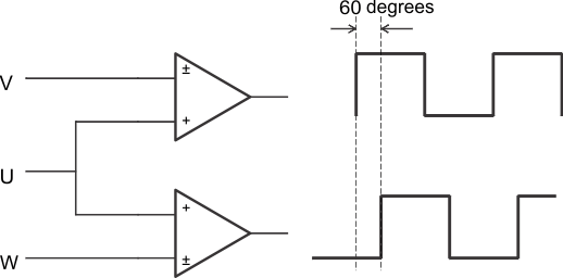 Figure 14. Initial Speed Detect Function
If the UW comparator output is lagging the UV comparator by 60°, the motor is spinning forward. If the UW comparator output is leading the UV comparator by 60°, the motor is spinning in reverse.
The motor speed is determined by measuring the time between two rising edges of either of the comparators.
If neither of the comparator outputs toggles for a given amount of time, the condition is defined as stationary. The amount of time can be programmed by setting the register bits ISDThr[1:0].
8.4.3.2 Motor Resynchronization
The resynchronize function works when the ISD function is enabled and determines that the initial state of the motor is spinning in the forward direction. The speed and position information measured during ISD are used to initialize the drive state of the DRV10983-Q1 device, which can transition directly into the closed-loop running state without needing to stop the motor.
8.4.3.3 Reverse Drive
The ISD function measures the initial speed and the initial position; the DRV10983-Q1 reverse drive function acts to reverse accelerate the motor through zero speed and to continue accelerating until the closed loop threshold is reached (see Figure 15). If the reverse speed is greater than the threshold configured in RvsDrThr[1:0], then the DRV10983-Q1 device waits until the motor coasts to a speed that is less than the threshold before driving the motor to reverse accelerate.
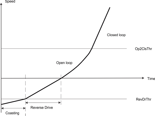 Figure 15. Reverse Drive Function
Reverse drive is suitable for applications where the load condition is light at low speed and relatively constant and where the reverse speed is low (that is, a fan motor with little friction). For other load conditions, the motor brake function provides a method for helping force a motor which is spinning in the reverse direction to stop spinning before a normal start-up sequence.
8.4.3.4 Motor Brake
The motor brake function can be used to stop the spinning motor before attempting to start the motor. The brake is applied by turning on all three of the low-side driver FETs.
Brake is enabled by configuring a non-zero BrkDoneThr[2:0]. Brake is applied for a time configured by BrkDoneThr[2:0] (forward or reverse). After the motor is stopped, the motor position is unknown. To proceed with restarting in the correct direction, the IPD or align-and-go algorithm must be implemented. The motor start sequence is the same as it would be for a motor starting in the stationary condition.
The motor brake function can be disabled. The motor skips the brake state and attempts to spin the motor as if it were stationary. If this happens while the motor is spinning in either direction, the start-up sequence may not be successful.
8.4.3.5 Motor Initialization
8.4.3.5.1 Align
The DRV10983-Q1 device aligns a motor by injecting dc current through a particular phase pattern which is current flowing into phase V, flowing out from phase W for a certain time (configured by AlignTime[2:0]). The current magnitude is determined by OpenLCurr[1:0]. The motor should be aligned at the known position.
The time of align affects the start-up timing (see Start-Up Timing). A bigger-inertia motor requires longer align time.
8.4.3.5.2 IPD
The inductive sense method is used to determine the initial position of the motor when IPD is enabled. IPD is enabled by selecting IPDCurrThr[3:0] to any value other than 0000.
IPD can be used in applications where reverse rotation of the motor is unacceptable. Because IPD is not required to wait for the motor to align with the commutation, it can allow for a faster motor start sequence. IPD works well when the inductance of the motor varies as a function of position. Because it works by pulsing current to the motor, it can generate acoustics which must be taken into account when determining the best start method for a particular application.
8.4.3.5.2.1 IPD Operation
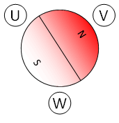
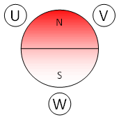
The IPD operates by sequentially applying voltage across two of the three motor phases according to the following sequence: VW WV UV VU WU UW (see Figure 16). When the current reaches the threshold configured in IPDCurrThr[3:0], the voltage across the motor is stopped. The DRV10983-Q1 device measures the time it takes from when the voltage is applied until the current threshold is reached. The time varies as a function of the inductance in the motor windings. The state with the shortest time represents the state with the minimum inductance. The minimum inductance is because of the alignment of the north pole of the motor with this particular driving state.
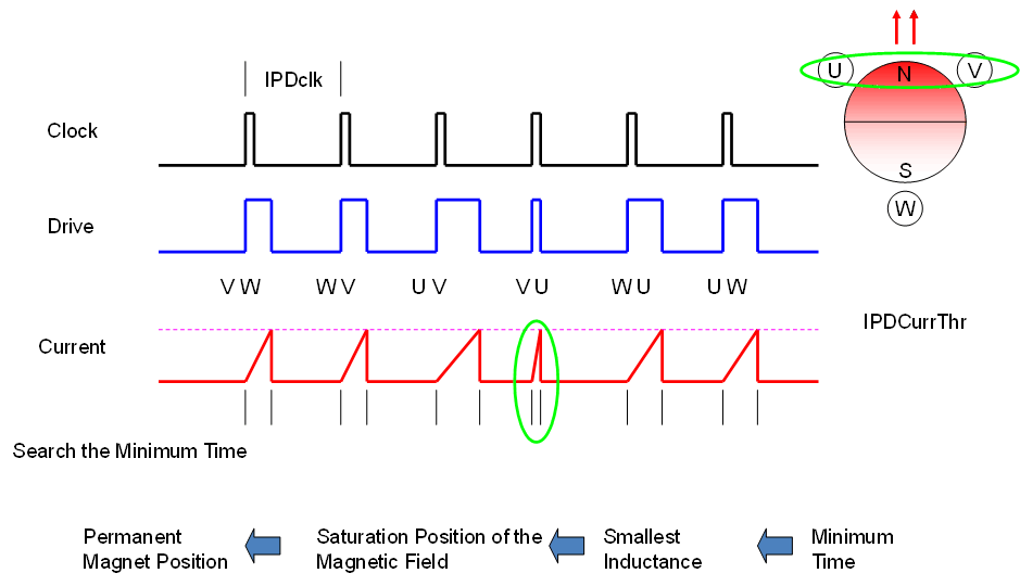 Figure 16. IPD Function
8.4.3.5.2.2 IPD Release Mode
Two options are available for stopping the voltage applied to the motor when the current threshold is reached. If IPDRlsMd = 0, the recirculate mode is selected. The low-side (S6) MOSFET remains on to allow the current to recirculate between the MOSFET (S6) and body diode (S2) (see Figure 17). If IPDRlsMd = 1, the tri-state mode is selected. Both the high-side (S1) and low-side (S6) MOSFETs are turned off and the current flies back across the body diodes into the power supply (see Figure 18).
In the high-impedance state, the phase current has a faster settle-down time, but that could result in a surge on VCC. Manage this with appropriate selection of either a clamp circuit or by providing sufficient capacitance between VCC and GND. If the voltage surge cannot be contained and if it is unacceptable for the application, then select the recirculate mode. When selecting the recirculate mode, select the IPDClk[1:0] bits to give the current in the motor windings enough time to decay to 0.
 Figure 17. IPD Release Mode 0
 Figure 18. IPD Release Mode 1
8.4.3.5.2.3 IPD Advance Angle
After the initial position is detected, the DRV10983-Q1 device begins driving the motor at an angle specified by IPDAdvcAgl[1:0].
Advancing the drive angle anywhere from 0° to 180° results in positive torque. Advancing the drive angle by 90° results in maximum initial torque. Applying maximum initial torque could result in uneven acceleration to the rotor. Select the IPDAdvcAgl[1:0] to allow for smooth acceleration in the application (see Figure 19).
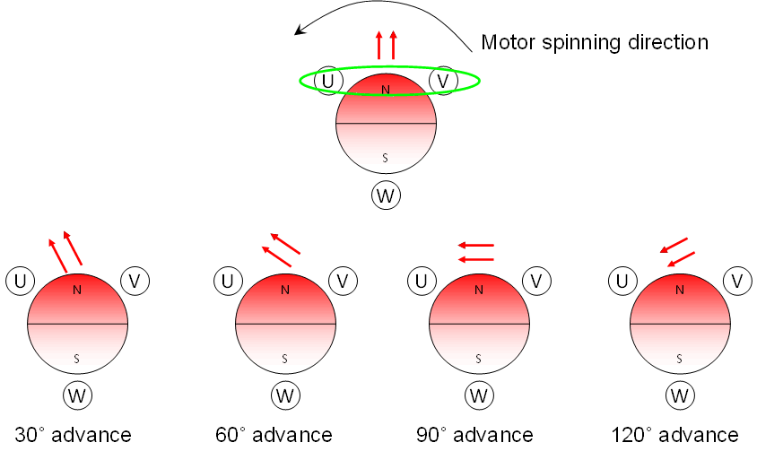 Figure 19. IPD Advance Angle
8.4.3.5.3 Motor Start
After it is determined that the motor is stationary and after completing the motor initialization with either align or IPD, the DRV10983-Q1 device begins to accelerate the motor. This acceleration is accomplished by applying a voltage determined by the open-loop current setting (OpenLCurr[1:0]) to the appropriate drive state and by increasing the rate of commutation without regard to the real position of the motor (referred to as open-loop operation). The function of the open-loop operation is to drive the motor to a minimum speed so that the motor generates sufficient BEMF to allow the commutation control logic to accurately drive the motor.
Table 5 lists the configuration options that can be set in register to optimize the initial motor acceleration stage for different applications.
Table 5. Configuration Options for Controlling Open-Loop Motor Start
| DESCRIPTION | REG. NAME | CONFIGURATION BITS | MIN. VALUE | MAX. VALUE |
|---|---|---|---|---|
| Open- to closed-loop threshold | CONFIG4 | Op2ClsThr[4:0] | 0.8 Hz | 204.8 Hz |
| Align time | CONFIG4 | AlignTime[2:0] | 40 ms | 5.3 s |
| First-order accelerate | CONFIG4 | StAccel[2:0] | 0.019 Hz/s | 76 Hz/s |
| Second-order accelerate | CONFIG4 | StAccel2[2:0] | 0.0026 Hz/s2 | 57 Hz/s2 |
| Open-loop current setting | CONFIG3 | OpenLCurr[1:0] | 200 mA | 1.6 A |
| Align current setting | 150 mA | 1.2 A | ||
| Open-loop current ramping | CONFIG3 | OpLCurrRt[2:0] | 0.023 VCC/s | 6 VCC/s |
8.4.3.6 Start-Up Timing
Start-up timing is determined by the align and accelerate time. The align time can be set by AlignTime[2:0]. The accelerate time is defined by the open-to-closed loop threshold Op2ClsThr[4:0] along with the first-order StAccel[2:0](A1) and second-order StAccel2[2:0](A2) accelerate rates. Figure 20 shows the motor start-up process.
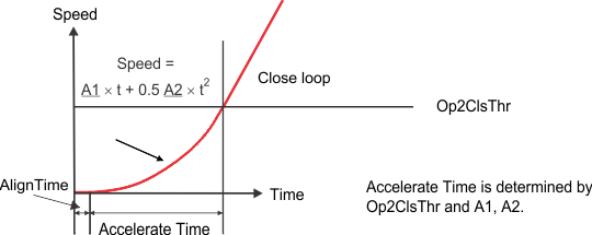 Figure 20. Motor Start-Up Process
Select the first-order and second-order accelerate rates to allow the motor to reliably accelerate from zero velocity up to the closed-loop threshold in the shortest time possible. Using a slow accelerate rate during the first order accelerate stage can help improve reliability in applications where it is difficult to accurately initialize the motor with either align or IPD.
Select the open-to-closed loop threshold to allow the motor to accelerate to a speed that generates sufficient BEMF for closed-loop control. This is determined by the velocity constant of the motor based on the relationship described in Equation 2.
8.4.4 Align Current
During the align state, the measured align current is dependent on actual motor resistance and rDS(on) of the internal FETs. The relationship between measured align current and configured align current is derived from actual motor resistance, configured motor resistance and rDS(on).

where
- AlignCurrent_Measured is the actual align current measured during the align state
- AlignCurrent_Configured is the align current configured by OpenLCurr[1:0]
- Rmotor is the actual motor resistance
- rDS(on) is the resistance between the drain and source of the FETs during the on-state
- Rm is configured by Rm[6:0]
8.4.5 Start-Up Current Setting
The start-up current setting is to control the peak start-up during open loop. During open-loop operation, it is desirable to control the magnitude of drive current applied to the motor. This is helpful in controlling and optimizing the rate of acceleration. The limit takes effect during reverse drive, align, and acceleration.
The start current is set by programming the OpenLCurr[1:0] bits. The current should be selected to allow the motor to reliably accelerate to the handoff threshold. Heavier loads may require a higher current setting, but it should be noted that the rate of acceleration is limited by the acceleration rate (StAccel[2:0], StAccel2[2:0]). If the motor is started with more current than necessary to reliably reach the handoff threshold, it results in higher power consumption.
The start current is controlled based on the relationship shown in Equation 4 and Figure 21. The duty cycle applied to the motor is derived from the calculated value for ULimit and the magnitude of the supply voltage, VCC, as well as the drive state of the motor.

where
- ILimit is configured by OpenLCurr[1:0]
- Rm is configured by Rm[6:0]
- Speed is variable based motor’s open loop acceleration profile
- Kt is configured by Kt[6:0]
 Figure 21. Motor Start-Up Current
8.4.5.1 Start-Up Current Ramp-Up
A fast change in the applied drive current may result in a sudden change in the driving torque. In some applications, this could result in acoustic noise. To avoid this, the DRV10983-Q1 device allows the option of limiting the rate at which the current is applied to the motor. OpLCurrRt[2:0] sets the maximum voltage ramp-up rate that is applied to the motor. The waveforms in Figure 22 show how this feature can be used to gradually ramp the current applied to the motor.
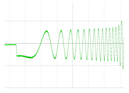 |
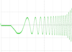 |
| Start driving with fast current ramp | Start driving with slow current ramp |
8.4.6 Closed Loop
In closed loop operation, the DRV10983-Q1 device continuously samples the current in the U phase of the motor and uses this information to estimate the BEMF voltage that is present. The drive state of the motor is controlled based on the estimated BEMF voltage.
8.4.6.1 Half-Cycle Control and Full-Cycle Control
The estimated BEMF used to control the drive state of the motor has two zero-crosses every electrical cycle. The DRV10983-Q1 device can be configured to update the drive state either once every electrical cycle or twice for every electrical cycle. When AdjMode is programmed to 1, half-cycle adjustment is applied. The control logic is triggered at both the rising edge and falling edge. When AdjMode is programmed to 0, full-cycle adjustment is applied. The control logic is triggered only at the rising edge (see Figure 23).
Half-cycle adjustment provides a faster response when compared with full-cycle adjustment. Use half-cycle adjustment whenever the application requires operation over large dynamic loading conditions. Use the full-cycle adjustment for low-current (<1 A) applications because it offers more tolerance for current-measurement offset errors.
 Figure 23. Closed-Loop Control Commutation-Adjustment Mode
8.4.6.2 Analog-Mode Speed Control
The SPEED input pin can be configured to operate as an analog input (SpdCtrlMd = 0).
When configured for analog mode, the voltage range on the SPEED pin can be varied from 0 to V3P3. If
SPEED > VANA_FS, the speed command is maximum. If VANA_ZS ≤ SPEED < VANA_FS the speed command changes linearly according to the magnitude of the voltage applied at the SPEED pin. If SPEED < VANA_ZS the speed command is to stop the motor. Figure 24 shows the speed command when operating in analog mode.
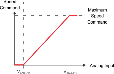 Figure 24. Analog-Mode Speed Command
8.4.6.3 Digital PWM-Input-Mode Speed Control
If SpdCtrlMd = 1, the SPEED input pin is configured to operate as a PWM-encoded digital input. The PWM duty cycle applied to the SPEED pin can be varied from 0 to 100%. The speed command is proportional to the PWM input duty cycle. The speed command stops the motor when the PWM input keeps at 0 for tEN_SL_SB (see Figure 25).
The frequency of the PWM input signal applied to the SPEED pin is defined as fPWM. This is the frequency the device can accept to control motor speed. It does not correspond to the PWM output frequency that is applied to the motor phase. The PWM output frequency can be configured to be either 25 kHz when the PWMFreq bit is set to 0 or to 50 kHz when PWMFreq bit is set to 1.
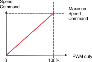 Figure 25. PWM-Mode Speed Command
8.4.6.4 I2C-Mode Speed Control
The DRV10983-Q1 device can also command the speed through the I2C serial interface. To enable this feature, the OverRide bit is set to 1. When the DRV10983-Q1 device is configured to operate in I2C mode, it ignores the signal applied to the SPEED pin.
The speed command can be set by writing the SpdCtrl[8:0] bits. The 9-bit SpdCtrl [8:0] located in the SpeedCtrl registers is used to set the peak amplitude voltage applied to the motor. The maximum speed command is set when SpdCtrl [8:0] is set to 0x1FF (511).
8.4.6.5 Closed-Loop Accelerate
To prevent sudden changes in the torque applied to the motor which could result in acoustic noise, the DRV10983-Q1 device provides the option of limiting the maximum rate at which the speed command changes. ClsLpAccel[2:0] can be programmed to set the maximum rate at which the speed command changes (shown in Figure 26).
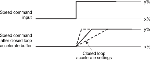 Figure 26. Closed Loop Accelerate
8.4.6.6 Control Coefficient
The DRV10983-Q1 device continuously measures the motor current and uses this information to control the drive state of the motor when operating in closed-loop mode. In applications where noise makes it difficult to control the commutation optimally, the CtrlCoef[1:0] can be used to attenuate the feedback used for closed-loop control. The loop is less reactive to the noise on the feedback and provides for a smoother output.
8.4.6.7 Commutation Control Advance Angle
To achieve the best efficiency, it is often desirable to control the drive state of the motor so that the motor phase current is aligned with the motor BEMF voltage.
To align the motor phase current with the motor BEMF voltage, consider the inductive effect of the motor. The voltage applied to the motor should be applied in advance of the motor BEMF voltage (see Figure 27). The DRV10983-Q1 device provides configuration bits for controlling the time (tadv) between the driving voltage and BEMF.
For motors with salient pole structures, aligning the motor BEMF voltage with the motor current may not achieve the best efficiency. In these applications, the timing advance should be adjusted accordingly. Accomplish this by operating the system at constant speed and load conditions and by adjusting tadv until the minimum current is achieved.
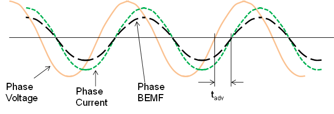 Figure 27. Advance Time (tadv) Definition
The DRV10983-Q1 device has two options for adjusting the motor commutate advance time. When CommAdvMode = 0, mode 0 is selected. When CommAdvMode = 1, mode 1 is selected.
Mode 0: tadv is maintained to be a fixed time relative to the estimated BEMF zero cross as determined by Equation 5.
Mode 1: tadv is maintained to be a variable time relative to the estimated BEMF zero cross as determined by Equation 6.
where
- U is the phase voltage amplitude
- BEMF is phase BEMF amplitude
tSETTING (in µs) is determined by the configuration of the TCtrlAdvShift [2:0] and TCtrlAdvValue [3:0] bits as defined in Equation 7. For convenience, the available tSETTING values are provided in Table 6.
Table 6. Configuring Commutation Advance Timing by Adjusting tSETTING
| TCtrlAdv [6:0] {TCtrlAdvShift[2:0], TCtrlAdvValue[3:0]} |
tSETTING (µs) | TCtrlAdv [6:0] {TCtrlAdvShift[2:0], TCtrlAdvValue[3:0]} |
tSETTING (µs) | TCtrlAdv [6:0] {TCtrlAdvShift[2:0], TCtrlAdvValue[3:0]} |
tSETTING (µs) | |||
|---|---|---|---|---|---|---|---|---|
| Binary | Hex | Binary | Hex | Binary | Hex | |||
| 000 0000 | 0x00 | 0.0 | 010 1000 | 0x28 | 80 | 101 1000 | 0x58 | 640 |
| 000 0001 | 0x01 | 2.5 | 010 1001 | 0x29 | 90 | 101 1001 | 0x59 | 720 |
| 000 0010 | 0x02 | 5 | 010 1010 | 0x2A | 100 | 101 1010 | 0x5A | 800 |
| 000 0011 | 0x03 | 7.5 | 010 1011 | 0x2B | 110 | 101 1011 | 0x5B | 880 |
| 000 0100 | 0x04 | 10 | 010 1100 | 0x2C | 120 | 101 1100 | 0x5C | 960 |
| 000 0101 | 0x05 | 12.5 | 010 1101 | 0x2D | 130 | 101 1101 | 0x5D | 1040 |
| 000 0110 | 0x06 | 15 | 010 1110 | 0x2E | 140 | 101 1110 | 0x5E | 1120 |
| 000 0111 | 0x07 | 17.5 | 010 1111 | 0x2F | 150 | 101 1111 | 0x5F | 1200 |
| 000 1000 | 0x08 | 20 | 011 1000 | 0x38 | 160 | 110 1000 | 0x68 | 1280 |
| 000 1001 | 0x09 | 22.5 | 011 1001 | 0x39 | 170 | 110 1001 | 0x69 | 1440 |
| 000 1010 | 0x0A | 25 | 011 1010 | 0x3A | 200 | 110 1010 | 0x6A | 1600 |
| 000 1011 | 0x0B | 27.5 | 011 1011 | 0x3B | 220 | 110 1011 | 0x6B | 1760 |
| 000 1100 | 0x0C | 30 | 011 1100 | 0x3C | 240 | 110 1100 | 0x6C | 1920 |
| 000 1101 | 0x0D | 32.5 | 011 1101 | 0x3D | 260 | 110 1101 | 0x6D | 2080 |
| 000 1110 | 0x0E | 35 | 011 1110 | 0x3E | 280 | 110 1110 | 0x6E | 2240 |
| 000 1111 | 0x0F | 37.5 | 011 1111 | 0x3F | 300 | 110 1111 | 0x6F | 2400 |
| 001 1000 | 0x18 | 40 | 100 1000 | 0x48 | 320 | 111 1000 | 0x78 | 2560 |
| 001 1001 | 0x19 | 45 | 100 1001 | 0x49 | 360 | 111 1001 | 0x79 | 2880 |
| 001 1010 | 0x1A | 50 | 100 1010 | 0x4A | 400 | 111 1010 | 0x7A | 3200 |
| 001 1011 | 0x1B | 55 | 100 1011 | 0x4B | 440 | 111 1011 | 0x7B | 3520 |
| 001 1100 | 0x1C | 60 | 100 1100 | 0x4C | 480 | 111 1100 | 0x7C | 3840 |
| 001 1101 | 0x1D | 65 | 100 1101 | 0x4D | 520 | 111 1101 | 0x7D | 4160 |
| 001 1110 | 0x1E | 70 | 100 1110 | 0x4E | 560 | 111 1110 | 0x7E | 4480 |
| 001 1111 | 0x1F | 75 | 100 1111 | 0x4F | 600 | 111 1111 | 0x7F | 4800 |
8.4.7 Current Limit
The DRV10983-Q1 device has several current-limit modes to help ensure optimal control of the motor and to ensure safe operation. The various current-limit modes are listed in Table 7. Acceleration current limit is used to provide a means of controlling the amount of current delivered to the motor. This is useful when the system needs to limit the amount of current pulled from the power supply during motor start-up. The lock-detection current limit is a configurable threshold that can be used to limit the current applied to the motor. Overcurrent protection is used to protect the device; therefore, it cannot be disabled or configured to a different threshold. The current-limit modes are described in the following sections.
Table 7. DRV10983-Q1 Current-Limit Modes
| CURRENT LIMIT MODE | SITUATION | ACTION | FAULT DIAGNOSIS |
|---|---|---|---|
| Acceleration current limit | Motor start | Limit the output voltage amplitude | No fault |
| Lock-detection current limit | Motor locked | Stop driving the motor and enter the lock state | Mechanical rotation error |
| Overcurrent shutdown | Short circuit | Stop driving the motor and enter the lock state | Circuit connection |
8.4.7.1 Acceleration Current Limit
The acceleration current limit limits the voltage applied to the motor to prevent the current from exceeding the programmed threshold. The acceleration current limit threshold is configured by writing the SWiLimitThr[3:0] bits to select ILIMIT. The acceleration current limit does not use a direct measurement of current. It uses the programmed motor resistance, Rm, and programmed motor velocity constant, Kt, to limit the voltage applied to the motor, U, as shown in Figure 28 and Equation 8.
When the acceleration current limit is active, it does not stop the motor from spinning nor does it trigger a fault. The functionality of the acceleration current limit is only available in closed-loop control.
 Figure 28. Acceleration Current Limit
8.4.8 Lock Detect and Fault Handling
The DRV10983-Q1 device provides several options for determining if the motor becomes locked as a result of some external torque. Five lock-detect schemes work together to ensure the lock condition is detected quickly and reliably. Figure 29 shows the logic which integrates the various lock-detect schemes. When a lock condition is detected, the DRV10983-Q1 device takes action to prevent continuously driving the motor in order to prevent damage to the system or the motor.
In addition to detecting if there is a locked motor condition, the DRV10983-Q1 device also identifies and takes action if there is no motor connected to the system.
Each of the five lock-detect schemes and the no-motor detection can be disabled by respective register bits LockEn[5:0].
When a lock condition is detected, the FaultReg register provides an indication of which of the six different conditions was detected on Lock5 to Lock0. These bits are reset when the motor restarts. The bits in the FaultReg register are set even if the lock detect scheme is disabled.
The DRV10983-Q1 device reacts to either locked-rotor or no-motor-connected conditions by putting the output drivers into a high-impedance state. To prevent the energy in the motor from pumping the supply voltage, the DRV10983-Q1 device incorporates an anti-voltage-surge (AVS) process whenever the output stages transition into the high-impedance state. The AVS function is described in Anti Voltage Supression Function. After entering the high-impedance state as a result of a fault condition, the system tries to restart after tLOCK_OFF.
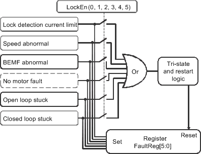 Figure 29. Lock Detect and Fault Diagnose
8.4.8.1 Lock0: Lock-Detection Current Limit Triggered
The lock-detection current-limit function provides a configurable threshold for limiting the current to prevent damage to the system. This is often tripped in the event of a sudden locked-rotor condition. The DRV10983-Q1 device continuously monitors the current in the low-side drivers as shown in Figure 30. If the current goes higher than the threshold configured by the HWiLimitThr[2:0] bits, then the DRV10983-Q1 device stops driving the motor by placing the output phases into a high-impedance state. The Lock0 bit is set and a lock condition is reported. It retries after tLOCK_OFF.
Set the lock-detection current limit to a higher value than the acceleration current limit.
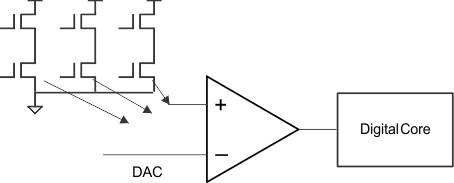 Figure 30. Lock-Detection Current Limit
8.4.8.2 Lock1: Abnormal Speed
If the motor is operating normally, the motor BEMF should always be less than the output amplitude. The DRV10983-Q1 device uses two methods of monitoring the BEMF in the system. The U phase current is monitored to maintain an estimate of BEMF based on the setting for Rm[6:0] {RmShift[2:0],RmValue[3:0]}. In addition, the BEMF is estimated based on the operation speed of the motor and the setting for Kt[6:0] {KtShift[2:0],KtValue[3:0]}. Figure 31 shows the method for using this information to detect a lock condition. If the motor BEMF is much higher than the output amplitude for a certain period of time, tLCK_ETR, it means the estimated speed is wrong, and the motor has gotten out of phase.
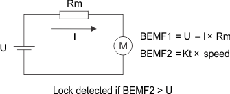 Figure 31. Lock Detection 1
8.4.8.3 Lock2: Abnormal Kt
For any given motor, the integrated value of BEMF during half of an electrical cycle is constant. The value is determined by the motor velocity constant (KtPH) (see Figure 32). The motor velocity constant is the same regardless of whether the motor is running fast or slow. This constant value is continuously monitored by calculation and used as a criterion to determine the motor lock condition, and is referred to as Ktc.
Based on the KtPH value programmed, create a range from Kt_low to Kt_high. If Ktc goes beyond the range for a certain period of time, tLCK_ETR, lock is detected. Kt_low and Kt_high are determined by KtLckThr[1:0] (see Figure 33).
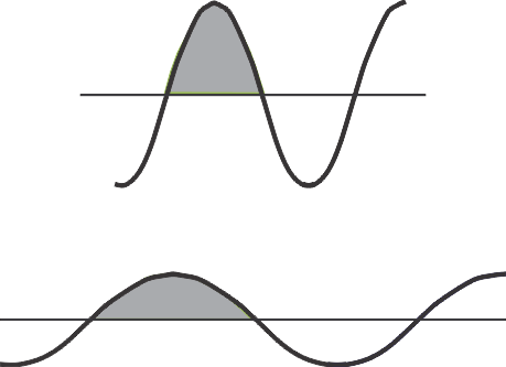 Figure 32. BEMF Integration
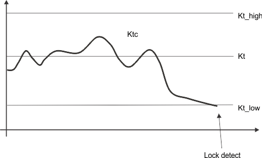 Figure 33. Abnormal-Kt Lock Detect
8.4.8.4 Lock3 (Fault3): No-Motor Fault
The phase U current is checked after transitioning from open loop to closed loop. If phase U current is not greater than 140 mA then the motor is not connected as shown in Figure 34. This condition is treated and reported as a fault.
 Figure 34. No Motor Error
8.4.8.5 Lock4: Open-Loop Motor-Stuck Lock
Lock4 is used to detect locked-motor conditions while the motor start sequence is in open loop.
For a successful startup, motor speed should be equal to the open-to-closed-loop handoff threshold when the motor is transitioning into closed loop. However, if the motor is locked, the motor speed is not able to match the open-loop drive rate.
If the motor BEMF is not detected for one electrical cycle after the open-loop drive rate exceeds the threshold, then the open loop was unsuccessful as a result of a locked-rotor condition.
8.4.8.6 Lock5: Closed Loop Motor Stuck Lock
If the motor suddenly becomes locked, motor speed and Ktc are not able to be refreshed because the BEMF zero cross of the motor may not appear after the lock. In this condition, lock can also be detected by the following scheme: if the current commutation period is 2× longer than the previous period.
8.4.9 Anti Voltage Supression Function
When a motor is driven, energy is transferred from the power supply into the motor. Some of this energy is stored in the form of inductive energy or as mechanical energy. The DRV10983-Q1 device includes circuits to prevent this energy from being returned to the power supply, which could result in pumping up the VCC voltage. This function is referred to as the AVS and acts to protect the DRV10983-Q1 device as well as other circuits that share the same VCC connection. Two forms of AVS protection are used to prevent both the mechanical energy and the inductive energy from being returned to the supply. Each of these modes can be independently disabled through the register configuration bits AVSMEn and AVSIndEn.
8.4.9.1 Mechanical AVS Function
If the speed command suddenly drops such that the BEMF voltage generated by the motor is greater than the voltage that is applied to the motor, then the mechanical energy of the motor is returned to the power supply and the VCC voltage surges. The mechanical AVS function works to prevent this from happening. The DRV10983-Q1 device buffers the speed command value and limits the resulting output voltage, UMIN, so that it is not less than the BEMF voltage of the motor. The BEMF voltage in the mechanical AVS function is determined using the programmed value for the motor Kt (Kt[6:0]) along with the speed. Figure 35 shows the criteria used by the mechanical AVS function.
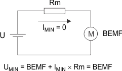 Figure 35. Mechanical AVS
The mechanical AVS function can operate in one of two modes, which can be configured by the register bit AVSMMd:
AVSMMd = 0 – AVS mode is always active to prevent the applied voltage from being less than the BEMF voltage.
AVSMMd = 1 – AVS mode becomes active when VCC reaches 24 V. The motor acts as a generator and returns energy into the power supply until VCC reaches 24 V. This mode can be used to enable faster deceleration of the motor in applications where returning energy to the power supply is allowed.
8.4.9.2 Inductive AVS Function
When the DRV10983-Q1 device transitions from driving the motor into a high-impedance state, the inductive current in the motor windings continues to flow and the energy returns to the power supply through the intrinsic body diodes in the FET output stage (see Figure 36).
 Figure 36. Inductive-Mode Voltage Surge
To prevent the inductive energy from being returned to the power supply, the DRV10983-Q1 system transitions from driving to a high-impedance state by first turning off the active high-side drivers, and then after a fixed period of time (BrkDoneThr[2:0]), turning off the low-side drivers (see Figure 37).
 Figure 37. Inductive AVS
In this example, current is applied to the motor through the high-side driver on phase U (S1) and returned through the low-side driver on phase W (S6). The high-side driver on phase U is turned off and after a period of time (to allow the inductive energy in the resulting LR circuit to decay) the low-side driver on phase W is turned off. If BrkDoneThr[2:0] = 000, no brake will be applied and the device will not protect from inductive energy even with the inductive AVS feature enabled.
8.4.10 PWM Output
The DRV10983-Q1 device has 32 options for PWM dead time. These options can be used to configure the time between one of the bridge FETs turning off and the complementary FET turning on. Deadtime[4:0] can be used to configure dead times between 40 and 1280 ns. Take care that the dead time is long enough to prevent the bridge FETs from shooting through.
The DRV10983-Q1 device offers two options for PWM switching frequency. When the configuration bit PWMFreq is set to 0, the output PWM frequency is 25 kHz, and when PWMFreq is set to 1, the output PWM frequency is 50 kHz.
8.4.11 FG Customized Configuration
The DRV10983-Q1 device provides information about the motor speed through the frequency generate (FG) pin. FG also provides information about the driving state of the DRV10983-Q1 device.
8.4.11.1 FG Output Frequency
The FG output frequency can be configured by FGcycle[3:0]. The default FG toggles once every electrical cycle (FGcycle = 0000). Many applications configure the FG output so that it provides two pulses for every mechanical rotation of the motor. The configuration bits provided in the DRV10983-Q1 device can accomplish this for 2-pole, 4-pole, 6-pole, and 8-pole motors up to 32-pole motors. This is illustrated in Figure 38 for 2, 4, 6, and 8-pole motors.
Figure 38 shows the DRV10983-Q1 device has been configured to provide FG pulses once every electrical cycle (4 poles), twice every three electrical cycles (6 poles), once every two electrical cycles (8 poles), and once every three electrical cycles (12 poles).
Note that when it is set to two FG pulses every three electrical cycles, the FG output is not 50% duty cycle. Motor speed is able to be measured by monitoring the rising edge of the FG output.
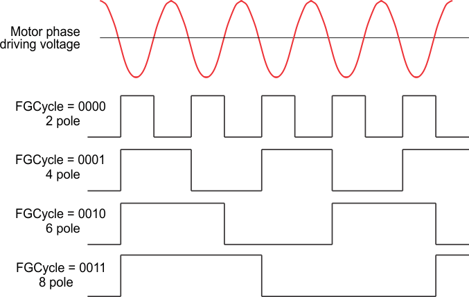 Figure 38. FG Frequency Divider
8.4.11.2 FG Open Loop and Lock Behavior
Note that the FG output reflects the driving state of the motor. During normal closed-loop behavior, the driving state and the actual state of the motor are synchronized. During open-loop acceleration, however, this may not reflect the actual motor speed. During a locked-motor condition, the FG output is driven high.
The DRV10983-Q1 device provides three options for controlling the FG output during open loop, as shown in Figure 39. The selection of these options is determined by the FGOLSel[1:0] setting.
- Option0: Open-loop, FG output based on driving frequency
- Option1: Open-loop, no FG output (keep high)
- Option2: FG output based on driving frequency at the first power-on startup, and no FG output (keep high) for any subsequent restarts
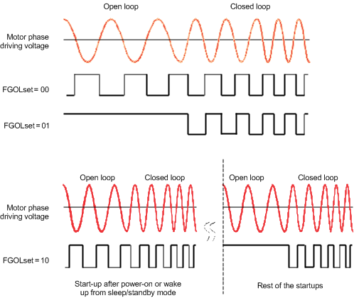 Figure 39. FG Behavior During Open Loop
8.4.12 Diagnostics and Visibility
The DRV10983-Q1 device offers extensive visibility into the motor system operation conditions stored in internal registers. This information can be monitored through the I2C interface. Information can be monitored relating to the device status, motor speed, supply voltage, speed command, motor phase-voltage amplitude, fault status, and others. The data is updated on the fly.
8.4.12.1 Motor-Status Readback
The motor FaultReg register provides information on overtemperature (OverTemp), overcurrent (OverCurr), and locked rotor (Lock0–Lock5).
8.4.12.2 Motor-Speed Readback
The motor operation speed is automatically updated in register MotorSpeed while the motor is spinning. The value is determined by the period for calculated BEMF zero crossings on phase U. The electrical speed of the motor is denoted as Velocity (Hz) and is calculated as shown in Equation 9.
As an example consider the following:
MotorSpeed = 0x01FF;
Velocity = 512 (0x01FF) / 10 = 51 Hz
For a 4-pole motor, this translates to: 
8.4.12.3 Motor Electrical-Period Readback
The motor-operation electrical period is automatically updated in register MotorPeriod while the motor is spinning. The electrical period is measured as the time between calculated BEMF zero crossings for phase U. The electrical period of the motor is denoted as tELE_PERIOD (µs) and is calculated as shown in Equation 10.
As an example consider the following:
MotorPeriod = 0x01FF;
tELE_PERIOD = 512 (0x01FF) × 10 = 5120 µs
The motor electrical period and motor speed satisfies the condition of Equation 11.
8.4.12.4 Motor Velocity Constant Read Back
For any given motor, the integrated value of BEMF during half of an electronic cycle is a constant, Ktc (see Lock2: Abnormal Kt ).
The integration of the motor BEMF is processed periodically (updated every electrical cycle) while the motor is spinning. The result is stored in register MotorKt.
The relationship is shown in .
8.4.12.5 Motor Estimated Position by IPD
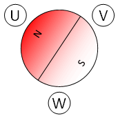
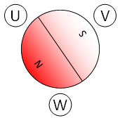
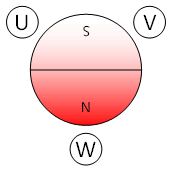
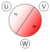
After inductive sense is executed, the rotor position is detected within 60 electrical degrees of resolution. The position is stored in register IPDPosition.
The value stored in IPDPosition corresponds to one of the six motor positions plus the IPD advance angle as shown in Table 8. For more information about IPD, see IPD.
Table 8. IPD Position Read Back
 |
 |
 |
 |
 |
 |
|
|---|---|---|---|---|---|---|
| Rotor position (°) | 0 | 60 | 120 | 180 | 240 | 300 |
| Data1 | 0 | 43 | 85 | 128 | 171 | 213 |
| IPD advance angle | 30 | 60 | 90 | 120 | ||
| Data2 | 22 | 44 | 63 | 85 | ||
| Register data | (Data1 + Data2) mod (256) | |||||
8.4.12.6 Supply-Voltage Readback
The power supply is monitored periodically during motor operation. This information is available in register SupplyVoltage. The power supply voltage is recorded as shown in Equation 13.
8.4.12.7 Speed-Command Readback
The DRV10983-Q1 device converts the various types of speed command into a speed command value (SpeedCmd) as shown in Figure 40. By reading SpeedCmd, the user can observe PWM input duty (PWM digital mode), analog voltage (analog mode), or I2C data (I2C mode). This value is calculated as shown in Equation 14.
Equation 14 shows how the speed command as a percentage can be calculated and set in SpeedCmd.
where
- DutySPEED = Speed command as a percentage
- SpeedCmd = Register value
8.4.12.8 Speed-Command Buffer Readback
If acceleration current limit and AVS are enabled, the PWM duty cycle output (read back at spdCmdBuffer) may not always match the input command (read back at SpeedCmd) shown in Figure 40. See Anti Voltage Supression Function and Current Limit.
By reading the value of spdCmdBuffer, the user can observe buffered speed command (output PWM duty cycle) to the motor.
Equation 15 shows how the buffered speed is calculated.
where
- DutyOUTPUT = The maximum duty cycle of the output PWM, which represents the output amplitude in percentage.
- spdCmdBuffer = Register value
 Figure 40. SpeedCmd and spdCmdBuffer Registers
8.4.12.9 Fault Diagnostics
8.5 Register Maps
8.5.1 I2C Serial Interface
The DRV10983-Q1 device provides an I2C slave interface with slave address 101 0010. TI recommends a pullup resistor of 4.7 kΩ to 3.3 V for I2C interface ports SCL and SDA. The protocol for the I2C interface is given in Figure 41.
 Figure 41. I2C Protocol
Seven read/write registers (0x30:0x36) are used to set motor speed and control device registers and EEPROM. Device operation status can be read back through nine read-only registers (0x0:0x08). Another seven EEPROM registers (0x90:0x96) can be accessed to program motor parameters and optimize the spin-up profile for the application.
8.5.2 Register Map
| REGISTER NAME | ADDR. | D15 | D14 | D13 | D12 | D11 | D10 | D9 | D8 |
|---|---|---|---|---|---|---|---|---|---|
| D7 | D6 | D5 | D4 | D3 | D2 | D1 | D0 | ||
| FaultReg (1)(2) | 0x00 | OverTemp | TempWarning | VCC_OV | VREG_OC | OverCurr | CP_UVLO | VREG_UVLO | VCC_UVLO |
| V3P3_UVLO | Reserved | Lock5 | Lock4 | Lock3 | Lock2 | Lock1 | Lock0 | ||
| MotorSpeed (1) | 0x01 | MotorSpeed[15:0] | |||||||
| MotorPeriod (1) | 0x02 | MotorPeriod[15:0] | |||||||
| MotorKt (1) | 0x03 | MotorKt[15:0] | |||||||
| MotorCurrent (1) | 0x04 | Reserved | MotorCurrent[10:8] | ||||||
| MotorCurrent[7:0] | |||||||||
| IPDPosition / SupplyVoltage (1) | 0x05 | IPDPosition[7:0] | |||||||
| SupplyVoltage[7:0] | |||||||||
| SpeedCmd / spdCmdBuffer(1) | 0x06 | SpeedCmd[7:0] | |||||||
| spdCmdBuffer[7:0] | |||||||||
| AnalogInLvl (1) | 0x07 | Reserved | commandSenseAdc[9:8] | ||||||
| commandSenseAdc[7:0] | |||||||||
| Device ID / Revision ID (1) | 0x08 | DieID[7:0] | |||||||
| RevisionID[7:0] | |||||||||
| SpeedCtrl (3) | 0x30 | OverRide | Reserved | SpeedCtrl[8] | |||||
| SpeedCtrl[7:0] | |||||||||
| EEPROM Programming1 (3) | 0x31 | ENPROGKEY[15:0] | |||||||
| EEPROM Programming2 (3) | 0x32 | Reserved | |||||||
| Reserved | eeReadyStatus | ||||||||
| EEPROM Programming3 (3) | 0x33 | Reserved | |||||||
| eeIndAddress[7:0] | |||||||||
| EEPROM Programming4 (3) | 0x34 | eeIndWData[15:0] | |||||||
| EEPROM Programming5 (3) | 0x35 | Reserved | ShadowRegEn | Reserved | eeRefresh | ||||
| Reserved | eeWRnEn | eeAccMode[1:0] | |||||||
| EEPROM Programming6 (3) | 0x36 | eeIndRData[15:0] | |||||||
| EECTRL | 0x60 | MTR_DIS | Reserved | ||||||
| Reserved | |||||||||
| CONFIG1 (4) | 0x90 | SSMConfig[1:0] | FGOLSel[1:0] | FGCycle[3:0] | |||||
| ClkCycleAdjust | RMShift[2:0] | RMValue[3:0] | |||||||
| CONFIG2 (4) | 0x91 | Reserved | KtShift[2:0] | KtValue[3:0] | |||||
| CommAdvMode | TCtrlAdvShift[2:0] | TCtrlAdvValue[3:0] | |||||||
| CONFIG3 (4) | 0x92 | ISDThr[1:0] | BrkCurrThrSel | BEMF_HYS | ISDEn | RvsDrEn | RvsDrThr[1:0] | ||
| OpenLCurr[1:0] | OpLCurrRt[2:0] | BrkDoneThr[2:0] | |||||||
| CONFIG4(4) | 0x93 | Reserved | AccelRangeSel | StAccel2[2:0] | StAccel[2:0] | ||||
| Op2ClsThr[4:0] | AlignTime[2:0] | ||||||||
| CONFIG5 (4) | 0x94 | OTWarning_ILimit[1:0] | LockEn5 | LockEn4 | LockEn3 | LockEn2 | LockEn1 | LockEn0 | |
| SwILimit[3:0] | HwILimit[2:0] | IPDasHwILimit | |||||||
| CONFIG6 (4) | 0x95 | SpdCtlrMd | PWMFreq | KtLckThr[1:0] | AvSIndEn | AVSMEn | AVSMMd | IPDRIsMd | |
| CLoopDis | ClsLpAccel[2:0] | DutyCycleLimit[1:0] | SlewRate[1:0] | ||||||
| CONFIG7 (4) | 0x96 | IPDAdvcAg[1:0] | IPDCurrThr[3:0] | IPDClk[1:0] | |||||
| Reserved | CtrlCoef[1:0] | DeadTime[4:0] | |||||||
Table 9. Default EEPROM Values
| ADDRESS | DEFAULT VALUE |
|---|---|
| 0x90 | 0x1048 |
| 0x91 | 0x2F3B |
| 0x92 | 0x0050 |
| 0x93 | 0x1B8A |
| 0x94 | 0x3FAF |
| 0x95 | 0x3C43 |
| 0x96 | 0x016A |
8.5.3 Register Descriptions
Table 10. Access Type Codes
| ACCESS TYPE | CODE | DESCRIPTION |
|---|---|---|
| READ TYPE | ||
| R | R | Read |
| WRITE TYPE | ||
| W | W | Write |
| W1C | W 1C |
Write 1 to clear |
| RESET OR DEFAULT VALUE | ||
| -n | Value after reset or the default value | |
8.5.3.1 FaultReg Register (address = 0x00) [reset = 0x00]
| 15 | 14 | 13 | 12 | 11 | 10 | 9 | 8 |
| OverTemp | TempWarning | VCC_OV | VREG_OC | OverCurr | CP_UVLO | VREG_UVLO | VCC_UVLO |
| R/W1C-0 | R//W1C-0 | R/W1C-0 | R/W1C-0 | R/W1C-0 | R/W1C-0 | R/W1C-0 | R/W1C-0 |
| 7 | 6 | 5 | 4 | 3 | 2 | 1 | 0 |
| V3P3_UVLO | Reserved | Lock5 | Lock4 | Lock3 | Lock2 | Lock1 | Lock0 |
| R/W1C-0 | R/W1C-0 | R/W1C-0 | R/W1C-0 | R/W1C-0 | R/W1C-0 | R/W1C-0 | R/W1C-0 |
Table 11. FaultReg Register Field Descriptions
| Bit | Field | Type | Reset | Description |
|---|---|---|---|---|
| 15 | OverTemp | R//W1C | 0 |
Bit to indicate device temperature is over the limit. |
| 14 | TempWarning | R/W1C | 0 | Bit to indicate device temperature is over the warning limit. |
| 13 | VCC_OV | R/W1C | 0 | Bit to indicate the supply voltage is above the upper limit. |
| 12 | VREG_OC | R/W1C | 0 | Bit to indicate that the switching regulator is in an overcurrent condition. |
| 11 | OverCurr | R/W1C | 0 | Bit to indicate that an overcurrent event happened. |
| 10 | CP_UVLO | R/W1C | 0 | Bit to indicate that the charge pump is in an undervoltage fault condition. |
| 9 | VREG_UVLO | R/W1C | 0 | Bit to indicate that the switching regulator (VREG) is in an undervoltage fault condition. |
| 8 | VCC_UVLO | R/W1C | 0 | Bit to indicate that the supply (VCC) is in an undervoltage fault condition. |
| 7 | V3P3_UVLO | R/W1C | 0 | Bit to indicate that the 3.3 V LDO regulator is in an undervoltage fault condition. |
| 6 | Reserved | R/W1C | 0 | Do not access this bit. |
| 5 | Lock5 | R/W1C | 0 | Stuck in closed loop fault |
| 4 | Lock4 | R/W1C | 0 | Stuck in open loop fault |
| 3 | Lock3 | R/W1C | 0 | No motor fault |
| 2 | Lock2 | R/W1C | 0 | Kt abnormal fault |
| 1 | Lock1 | R/W1C | 0 | Speed abnormal fault |
| 0 | Lock0 | R/W1C | 0 | Hardware current-limit fault |
8.5.3.2 MotorSpeed Register (address = 0x01) [reset = 0x00]
| 15 | 14 | 13 | 12 | 11 | 10 | 9 | 8 |
| MotorSpeed[15] | MotorSpeed[14] | MotorSpeed[13] | MotorSpeed[12] | MotorSpeed[11] | MotorSpeed[10] | MotorSpeed[9] | MotorSpeed[8] |
| R-0 | R-0 | R-0 | R-0 | R-0 | R-0 | R-0 | R-0 |
| 7 | 6 | 5 | 4 | 3 | 2 | 1 | 0 |
| MotorSpeed[7] | MotorSpeed[6] | MotorSpeed[5] | MotorSpeed[4] | MotorSpeed[3] | MotorSpeed[2] | MotorSpeed[1] | MotorSpeed[0] |
| R-0 | R-0 | R-0 | R-0 | R-0 | R-0 | R-0 | R-0 |
Table 12. MotorSpeed Register Field Descriptions
| Bit | Field | Type | Reset | Description |
|---|---|---|---|---|
| 15:0 | MotorSpeed[15:0] | R | 0x00 | 16-bit value indicating the motor speed. Motor speed in Hz = MotorSpeed[15:0] / 10 |
8.5.3.3 MotorPeriod Register (address = 0x02) [reset = 0x00]
| 15 | 14 | 13 | 12 | 11 | 10 | 9 | 8 |
| MotorPeriod[15] | MotorPeriod[14] | MotorPeriod[13] | MotorPeriod[12] | MotorPeriod[11] | MotorPeriod[10] | MotorPeriod[9] | MotorPeriod[8] |
| R-0 | R-0 | R-0 | R-0 | R-0 | R-0 | R-0 | R-0 |
| 7 | 6 | 5 | 4 | 3 | 2 | 1 | 0 |
| MotorPeriod[7] | MotorPeriod[6] | MotorPeriod[5] | MotorPeriod[4] | MotorPeriod[3] | MotorPeriod[2] | MotorPeriod[1] | MotorPeriod[0] |
| R-0 | R-0 | R-0 | R-0 | R-0 | R-0 | R-0 | R-0 |
Table 13. MotorPeriod Register Field Descriptions
| Bit | Field | Type | Reset | Description |
|---|---|---|---|---|
| 15:0 | MotorPeriod[15:0] | R | 0x00 | 16-bit value indicating the motor period. Motor period = MotorPeriod[15:0] × 10 = period in μs |
8.5.3.4 MotorKt Register (address = 0x03) [reset = 0x00]
| 15 | 14 | 13 | 12 | 11 | 10 | 9 | 8 |
| MotorKt[15] | MotorKt[14] | MotorKt[13] | MotorKt[12] | MotorKt[11] | MotorKt[10] | MotorKt[9] | MotorKt[8] |
| R-0 | R-0 | R-0 | R-0 | R-0 | R-0 | R-0 | R-0 |
| 7 | 6 | 5 | 4 | 3 | 2 | 1 | 0 |
| MotorKt[7] | MotorKt[6] | MotorKt[5] | MotorKt[4] | MotorKt[3] | MotorKt[2] | MotorKt[1] | MotorKt[0] |
| R-0 | R-0 | R-0 | R-0 | R-0 | R-0 | R-0 | R-0 |
Table 14. MotorKt Register Field Descriptions
| Bit | Field | Type | Reset | Description |
|---|---|---|---|---|
| 15:0 | MotorKt[15:0] | R | 0x00 | 16-bit value indicating the motor measured velocity constant. Ktc (V/Hz) = {MotorKt[15:0]} / 2 / 1090 |
8.5.3.5 MotorCurrent Register (address = 0x04) [reset = 0x00]
| 15 | 14 | 13 | 12 | 11 | 10 | 9 | 8 |
| Reserved | Reserved | Reserved | Reserved | Reserved | MotorCurrent[10] | MotorCurrent[9] | MotorCurrent[8] |
| R-0 | R-0 | R-0 | R-0 | R-0 | R-0 | R-0 | R-0 |
| 7 | 6 | 5 | 4 | 3 | 2 | 1 | 0 |
| MotorCurrent[7] | MotorCurrent[6] | MotorCurrent[5] | MotorCurrent[4] | MotorCurrent[3] | MotorCurrent[2] | MotorCurrent[1] | MotorCurrent[0] |
| R-0 | R-0 | R-0 | R-0 | R-0 | R-0 | R-0 | R-0 |
Table 15. MotorCurrent Register Field Descriptions
| Bit | Field | Type | Reset | Description |
|---|---|---|---|---|
| 15:11 | Reserved | R | 0 | Do not access these bits. |
| 10:0 | MotorCurrent[10:0] | R | 0x00 | 11-bit value indicating the motor current. Current (A) = 3 × (MotorCurrent[10:0] –- 1023) / 2048 |
8.5.3.6 IPDPosition–SupplyVoltage Register (address = 0x05) [reset = 0x00]
| 15 | 14 | 13 | 12 | 11 | 10 | 9 | 8 |
| IPDPosition [7] | IPDPosition [6] | IPDPosition [5] | IPDPosition [4] | IPDPosition [3] | IPDPosition [2] | IPDPosition [1] | IPDPosition [0] |
| R-0 | R-0 | R-0 | R-0 | R-0 | R-0 | R-0 | R-0 |
| 7 | 6 | 5 | 4 | 3 | 2 | 1 | 0 |
| SupplyVoltage[7] | SupplyVoltage[6] | SupplyVoltage[5] | SupplyVoltage[4] | SupplyVoltage[3] | SupplyVoltage[2] | SupplyVoltage[1] | SupplyVoltage[0] |
| R-0 | R-0 | R-0 | R-0 | R-0 | R-0 | R-0 | R-0 |
Table 16. IPDPosition–SupplyVoltage Register Field Descriptions
| Bit | Field | Type | Reset | Description |
|---|---|---|---|---|
| 15:8 | IPDPosition [7:0] | R | 0x0 | 8-bit value indicating the estimated motor position during IPD plus the IPD advance angle (see Table 8) |
| 7:0 | SupplyVoltage[7:0] | R | 0x0 | 8-bit value indicating the supply voltage VPOWERSUPPLY (V) = SupplyVoltage[7:0] × 30 V / 255 For example, SupplyVoltage[7:0] = 0x67, VPOWERSUPPLY (V) = 0x67 (102) × 30 / 255 = 12 V |
8.5.3.7 SpeedCmd–spdCmdBuffer Register (address = 0x06) [reset = 0x00]
| 15 | 14 | 13 | 12 | 11 | 10 | 9 | 8 |
| SpeedCmd[7] | SpeedCmd[6] | SpeedCmd[5] | SpeedCmd[4] | SpeedCmd[3] | SpeedCmd[2] | SpeedCmd[1] | SpeedCmd[0] |
| R-0 | R-0 | R-0 | R-0 | R-0 | R-0 | R-0 | R-0 |
| 7 | 6 | 5 | 4 | 3 | 2 | 1 | 0 |
| spdCmdBuffer[[7] | spdCmdBuffer[[6] | spdCmdBuffer[[5] | spdCmdBuffer[[4] | spdCmdBuffer[[3] | spdCmdBuffer[[2] | spdCmdBuffer[[1] | spdCmdBuffer[[0] |
| R-0 | R-0 | R-0 | R-0 | R-0 | R-0 | R-0 | R-0 |
Table 17. SpeedCmd–spdCmdBuffer Register Field Descriptions
| Bit | Field | Type | Reset | Description |
|---|---|---|---|---|
| 15:8 | SpeedCmd[7:0] | R | 0x0 | 8-bit value indicating the speed command based on analog or PWMin or I2C. FF indicates 100% speed command. |
| 7:0 | spdCmdBuffer[7:0] | R | 0x0 | 8-bit value indicating the speed command after buffer output. FF indicates 100% speed command. |
8.5.3.8 AnalogInLvl Register (address = 0x07) [reset = 0x00]
| 15 | 14 | 13 | 12 | 11 | 10 | 9 | 8 |
| Reserved | Reserved | Reserved | Reserved | Reserved | Reserved | commandSnsADC[9] | commandSnsADCt[8] |
| R-0 | R-0 | R-0 | R-0 | R-0 | R-0 | R-0 | R-0 |
| 7 | 6 | 5 | 4 | 3 | 2 | 1 | 0 |
| commandSnsADC[7] | commandSnsADC[6] | commandSnsADC[5] | commandSnsADC[4] | commandSnsADC[3] | commandSnsADC[2] | commandSnsADC[1] | commandSnsADC[0] |
| R-0 | R-0 | R-0 | R-0 | R-0 | R-0 | R-0 | R-0 |
Table 18. AnalogInLvl Register Field Descriptions
| Bit | Field | Type | Reset | Description |
|---|---|---|---|---|
| 15:10 | Reserved | R | 0 | Do not access these bits. |
| 9:0 | commandSnsADC[9:0] | R | 0x00 | 10-bit value indicating the analog speed input converted to a digital word. AnalogSPEED (V) = AnalogInLvl × V3P3 / 1024 |
8.5.3.9 DeviceID–RevisionID Register (address = 0x08) [reset = 0x00]
| 15 | 14 | 13 | 12 | 11 | 10 | 9 | 8 |
| DieID[7] | DieID[6] | DieID[5] | DieID[4] | DieID[3] | DieID[2] | DieID[1] | DieID[0] |
| R-0 | R-0 | R-0 | R-0 | R-0 | R-0 | R-0 | R-0 |
| 7 | 6 | 5 | 4 | 3 | 2 | 1 | 0 |
| RevisionID[7] | RevisionID[6] | RevisionID[5] | RevisionID[4] | RevisionID[3] | RevisionID[2] | RevisionID[1] | RevisionID[0] |
| R-0 | R-0 | R-0 | R-0 | R-0 | R-0 | R-0 | R-0 |
Table 19. DeviceID–RevisionID Register Field Descriptions
| Bit | Field | Type | Reset | Description |
|---|---|---|---|---|
| 15:10 | DieID[7:0] | R | 0 | 8-bit unique device identification. |
| 9:0 | RevisionID[7:0] | R | 0x00 | 8-bit revision ID for the device 0000 0000 → REV A 0000 0001 → REV B ... |
8.5.3.10 DeviceID–RevisionID Register (address = 0x08) [reset = 0x00]
| 15 | 14 | 13 | 12 | 11 | 10 | 9 | 8 |
| DieID[7] | DieID[6] | DieID[5] | DieID[4] | DieID[3] | DieID[2] | DieID[1] | DieID[0] |
| R-0 | R-0 | R-0 | R-0 | R-0 | R-0 | R-0 | R-0 |
| 7 | 6 | 5 | 4 | 3 | 2 | 1 | 0 |
| RevisionID[7] | RevisionID[6] | RevisionID[5] | RevisionID[4] | RevisionID[3] | RevisionID[2] | RevisionID[1] | RevisionID[0] |
| R-0 | R-0 | R-0 | R-0 | R-0 | R-0 | R-0 | R-0 |
Table 20. DeviceID–RevisionID Register Field Descriptions
| Bit | Field | Type | Reset | Description |
|---|---|---|---|---|
| 15:8 | DieID[7:0] | R | 0x0 | 8-bit unique device identification. |
| 7:0 | RevisionID[7:0] | R | 0x0 | 8-bit revision ID for the device 0000 0000 → REV A 0000 0001 → REV B ... |
8.5.3.11 Unused Registers (addresses = 0x011 Through 0x2F)
Registers 0x09 through 0x2F are not used.
8.5.3.12 SpeedCtrl Register (address = 0x30) [reset = 0x00]
| 15 | 14 | 13 | 12 | 11 | 10 | 9 | 8 |
| OverRide | Reserved | Reserved | Reserved | Reserved | Reserved | Reserved | SpeedCtrl[8] |
| R/W-0 | R-0 | R-0 | R-0 | R-0 | R-0 | R-0 | R/W-0 |
| 7 | 6 | 5 | 4 | 3 | 2 | 1 | 0 |
| SpeedCtrl[7] | SpeedCtrl[6] | SpeedCtrl[5] | SpeedCtrl[4] | SpeedCtr[3] | SpeedCtrl[2] | SpeedCtrl[1] | SpeedCtrl[0] |
| R/W-0 | R/W-0 | R/W-0 | R/W-0 | R/W-0 | R/W-0 | R/W-0 | R/W-0 |
Table 21. SpeedCtrl Register Field Descriptions
| Bit | Field | Type | Reset | Description |
|---|---|---|---|---|
| 15 | OverRide | R/W | 0 | Used to control the SpdCtrl[8:0] bits. If OverRide = 1, the user can write the speed command directly through I2C. |
| 14:9 | Reserved | R | 0x0 | Do not access this bit. |
| 8:0 | SpeedCtrl[8:0] | R/W | 0x00 | 9-bit value used for the motor speed. If OverRide = 1, speed command can be written by the user through I2C. |
8.5.3.13 EEPROM Programming1 Register (address = 0x31) [reset = 0x00]
| 15 | 14 | 13 | 12 | 11 | 10 | 9 | 8 |
| ENPROGKEY [15] | ENPROGKEY [14] | ENPROGKEY [13] | ENPROGKEY [12] | ENPROGKEY [11] | ENPROGKEY [10] | ENPROGKEY [9] | ENPROGKEY [9] |
| R/W-0 | R/W-0 | R/W-0 | R/W-0 | R/W-0 | R/W-0 | R/W-0 | R/W-0 |
| 7 | 6 | 5 | 4 | 3 | 2 | 1 | 0 |
| ENPROGKEY [7] | ENPROGKEY [6] | ENPROGKEY [5] | ENPROGKEY [4] | ENPROGKEY [3] | ENPROGKEY [2] | ENPROGKEY [1] | ENPROGKEY [0] |
| R/W-0 | R/W-0 | R/W-0 | R/W-0 | R/W-0 | R/W-0 | R/W-0 | R/W-0 |
Table 22. EEPROM Programming1 Register Field Descriptions
| Bit | Field | Type | Reset | Description |
|---|---|---|---|---|
| 15:0 | ENPROGKEY[15:0] | R/W | 0x00 | EEPROM access key 0xCODE → access key for customer space; registers 0x90 to 0x96 |
8.5.3.14 EEPROM Programming2 Register (address = 0x32) [reset = 0x00]
| 15 | 14 | 13 | 12 | 11 | 10 | 9 | 8 |
| Reserved | Reserved | Reserved | Reserved | Reserved | Reserved | Reserved | Reserved |
| R-0 | R-0 | R-0 | R-0 | R-0 | R-0 | R-0 | R-0 |
| 7 | 6 | 5 | 4 | 3 | 2 | 1 | 0 |
| Reserved | Reserved | Reserved | Reserved | Reserved | Reserved | Reserved | eeReadyStatus |
| R-0 | R-0 | R-0 | R-0 | R-0 | R-0 | R-0 | R-0 |
Table 23. EEPROM Programming2 Register Field Descriptions
| Bit | Field | Type | Reset | Description |
|---|---|---|---|---|
| 15:1 | Reserved | R | 0x00 | Do not access these bits. |
| 0 | eeReadyStatus | R | 0 | EEPROM status bit. 0: EEPROM not ready for read/write access 1: EEPROM ready for read/write access |
8.5.3.15 EEPROM Programming3 Register (address = 0x33) [reset = 0x00]
| 15 | 14 | 13 | 12 | 11 | 10 | 9 | 8 |
| Reserved | Reserved | Reserved | Reserved | Reserved | Reserved | Reserved | Reserved |
| R-0 | R-0 | R-0 | R-0 | R-0 | R-0 | R-0 | R-0 |
| 7 | 6 | 5 | 4 | 3 | 2 | 1 | 0 |
| eeIndAddress [7] | eeIndAddress [6] | eeIndAddress [5] | eeIndAddress [4] | eeIndAddress [3] | eeIndAddress [2] | eeIndAddress [1] | eeIndAddress [0] |
| R-0 | R-0 | R-0 | R-0 | R-0 | R-0 | R-0 | R-0 |
Table 24. EEPROM Programming3 Register Field Descriptions
| Bit | Field | Type | Reset | Description |
|---|---|---|---|---|
| 15:8 | Reserved | R | 0x0 | Do not access these bits. |
| 7:0 | eeIndAddress[7:0] | R | 0x0 | EEPROM individual access address. Contents of this register define the address of EEPROM for the individual access operation. For example, for writing/reading CONFIG1 in individual access mode happens if eeIndAddress = 0x90. |
8.5.3.16 EEPROM Programming4 Register (address = 0x34) [reset = 0x00]
| 15 | 14 | 13 | 12 | 11 | 10 | 9 | 8 |
| eeIndWData [15] | eeIndWData [14] | eeIndWData [13] | eeIndWData [12] | eeIndWData [11] | eeIndWData [10] | eeIndWData[9] | eeIndWData[8] |
| R/W-0 | R/W-0 | R/W-0 | R/W-0 | R/W-0 | R/W-0 | R/W-0 | R/W-0 |
| 7 | 6 | 5 | 4 | 3 | 2 | 1 | 0 |
| eeIndWData[7] | eeIndWData[6] | eeIndWData[5] | eeIndWData[4] | eeIndWData[3] | eeIndWData[2] | eeIndWData[1] | eeIndWData[0] |
| R/W-0 | R/W-0 | R/W-0 | R/W-0 | R/W-0 | R/W-0 | R/W-0 | R/W-0 |
Table 25. EEPROM Programming4 Register Field Descriptions
| Bit | Field | Type | Reset | Description |
|---|---|---|---|---|
| 15:0 | eeIndWData[15:0] | R/W | 0x00 | EEPROM individual access write data Contents of this register are used to write to EEPROM data of the registers specified by eeIndAddress. |
8.5.3.17 EEPROM Programming5 Register (address = 0xYY) [reset = 0x00]
| 15 | 14 | 13 | 12 | 11 | 10 | 9 | 8 |
| Reserved | Reserved | Reserved | ShadowRegEn | Reserved | Reserved | Reserved | |
| R-0 | R-0 | R-0 | R/W-0 | R-0 | R-0 | R-0 | R-0 |
| 7 | 6 | 5 | 4 | 3 | 2 | 1 | 0 |
| Reserved | Reserved | Reserved | Reserved | Reserved | eeWRnEn | eeAccMode[1] | eeAccMode[0] |
| R-0 | R-0 | R-0 | R-0 | R-0 | R/W-0 | R/W-0 | R/W-0 |
Table 26. EEPROM Programming5 Register Field Descriptions
| Bit | Field | Type | Reset | Description |
|---|---|---|---|---|
| 15:13 | Reserved | R | 000 | Do not access these bits. |
| 12 | ShadowRegEn | R/W | 0 | Enable shadow register. 0 : Shadow register is not used. 1 : Shadow register values are used for device operation (EEPROM contents are ignored). I2C read returns the contents of the shadow registers. |
| 11:9 | Reserved | R | 000 | Do not access these bits. |
| 8 | eeRefresh | R/W | 0 | EEPROM refresh 0 : normal operation 1 : Sync shadow registers with contents of EEPROM. |
| 7:3 | Reserved | R | 0x0 | Do not access these bits. |
| 2 | eeWRnEn | R/W | 0 | EEPROM refresh 0 : Normal operation 1 : Sync shadow registers with contents of EEPROM. |
| 1:0 | eeAccMode[1:0] | R/W | 00 | EEPROM access mode 00 : EEPROM access disabled 01 : EEPROM individual access enabled 10 : EEPROM mass access enabled 11 : Do not access these bits. |
8.5.3.18 EEPROM Programming6 Register (address = 0x36) [reset = 0x00]
| 15 | 14 | 13 | 12 | 11 | 10 | 9 | 8 |
| eeIndRData[15] | eeIndRData[14] | eeIndRData[13] | eeIndRData[12] | eeIndRData[11] | eeIndRData[10] | eeIndRData[9] | eeIndRData[8] |
| R-0 | R-0 | R-0 | R-0 | R-0 | R-0 | R-0 | R-0 |
| 7 | 6 | 5 | 4 | 3 | 2 | 1 | 0 |
| eeIndRData[7] | eeIndRData[6] | eeIndRData[5] | eeIndRData[4] | eeIndRData[3] | eeIndRData[2] | eeIndRData[1] | eeIndRData[0] |
| R-0 | R-0 | R-0 | R-0 | R-0 | R-0 | R-0 | R-0 |
Table 27. EEPROM Programming6 Register Field Descriptions
| Bit | Field | Type | Reset | Description |
|---|---|---|---|---|
| 15:0 | eeIndRData[15:0] | R | 0x00 | EEPROM Individual Access Read Data Contents of this register reflect the value of EEPROM location accessed through the individual read. |
8.5.3.19 Unused Registers (addresses = 0x37 Through 0x5F)
Registers 0x37 through 0x5F are not used.
8.5.3.20 EECTRL Register (address = 0x60) [reset = 0x00]
| 15 | 14 | 13 | 12 | 11 | 10 | 9 | 8 |
| MTR_DIS | Reserved | Reserved | Reserved | Reserved | Reserved | Reserved | Reserved |
| W-0 | R-0 | R-0 | R-0 | R-0 | R-0 | R-0 | R-0 |
| 7 | 6 | 5 | 4 | 3 | 2 | 1 | 0 |
| Reserved | Reserved | Reserved | Reserved | Reserved | Reserved | Reserved | Reserved |
| R-0 | R-0 | R-0 | R-0 | R-0 | R-0 | R-0 | R-0 |
Table 28. EECTRL Register Field Descriptions
| Bit | Field | Type | Reset | Description |
|---|---|---|---|---|
| 15 | MTR_DIS | W | 0 | Control to disable motor without going to sleep. For use during EEPROM programming. This bit is write-only (cannot be read). 0: Motor control is enabled. 1: Motor control is disabled. |
| 14:0 | Reserved | R | 0x00 | Do not access these bits. |
8.5.3.21 Unused Registers (addresses = 0x61 Through 0x8F)
Registers 0x61 through 0x8F are not used.
8.5.3.22 CONFIG1 Register (address = 0x90) [reset = 0x00]
| 15 | 14 | 13 | 12 | 11 | 10 | 9 | 8 |
| SSMConfig[1] | SSMConfig[0] | FGOLSel[1] | FGOLSel[0] | FGCycle[3] | FGCycle[2] | FGCycle[1] | FGCycle[0] |
| R/W-0 | R/W-0 | R/W-0 | R/W-0 | R/W-0 | R/W-0 | R/W-0 | R/W-0 |
| 7 | 6 | 5 | 4 | 3 | 2 | 1 | 0 |
| ClkCycleAdjust | RMShift[2] | RMShift[1] | RMShift[0] | RMValue[3] | RMValue[2] | RMValue[1] | RMValue[0] |
| R/W-0 | R/W-0 | R/W-0 | R/W-0 | R/W-0 | R/W-0 | R/W-0 | R/W-0 |
Table 29. CONFIG1 Register Field Descriptions
| Bit | Field | Type | Reset | Description |
|---|---|---|---|---|
| 15:14 | SSMConfig[1:0] | R/W | 00 | Spread spectrum modulation control 00: No spread spectrum 01: ±5% dithering 1:0: ±10% dithering 11: ±15% dithering |
| 13:12 | FGOLSel[1:0] | R/W | 00 | FG open-loop output select 00: FG outputs in both open loop and closed loop 01: FG outputs only in closed loop 10: FG outputs closed loop and the first open loop 11: Reserved |
| 11:8 | FGCycle[3:0] | R/W | 0x0 | FG motor pole option n: FG output is electrical speed / (n + 1) 0: FG / 1 (2 pole) 1: FG / 2 (4 pole) 2: FG / 3 (6 pole) 3: FG / 4 (8 pole) ... 15: FG / 16 (32 pole) |
| 7 | ClkCycleAdjust | R/W | 0 | 0: Full-cycle adjust 1: Half-cycle adjust |
| 6:4 | RMShift[2:0] | R/W | 000 | Number of shift bits to determine the motor phase resistance. RM = RmValue << RmShift Rm' = (bin) {RPhase / 0.009615} After calculating Rm' value, split the value with shift number and significant number according the length of the Rm' value. If the length of Rm' is within 4 bits; RmValue[3:0] = Rm'; RmShift[2:0] = 000 If the length of Rm' is 5 bits; RmValue[3:0] = Rm'[4:1]; RmShift[2:0] = 001 and so on. |
| 3:0 | RMValue[3:0] | R/W | 0x0 | Significant portion of the motor resistor, used in conjunction with RmShift[2:0] |
8.5.3.23 CONFIG2 Register (address = 0x91) [reset = 0x00]
| 15 | 14 | 13 | 12 | 11 | 10 | 9 | 8 |
| Reserved | KtShift[2] | KtShift[1] | KtShift[0] | KtValue[3] | KtValue[2] | KtValue[1] | KtValue[0] |
| R-0 | R/W-0 | R/W-0 | R/W-0 | R/W-0 | R/W-0 | R/W-0 | R/W-0 |
| 7 | 6 | 5 | 4 | 3 | 2 | 1 | 0 |
| CommAdvMode | TCtrlAdvShift[2] | TCtrlAdvShift[1] | TCtrlAdvShift[0] | ||||
| R/W-0 | R/W-0 | R/W-0 | R/W-0 | R-0 | R-0 | R-0 | R-0 |
Table 30. CONFIG2 Register Field Descriptions
| Bit | Field | Type | Reset | Description |
|---|---|---|---|---|
| 15 | Reserved | R | 0 | Do not access this bit |
| 14:12 | KtShift[2:0] | R/W | 000 | Number of shift bits to determine the motor BEMF constant. Kt = KtValue << KtShift |
| 11:8 | KtValue[3:0] | R/W | 0x0 | |
| 7 | CommAdvMode | R/W | 0 | Commutation advance mode 0: Voltage advance is maintained at a fixed time(4) relative to the estimated BEMF. 1: Voltage advance is maintained at a variable time relative to the estimated BEMF based on: tadv = tsetting × (U-BEMF) / U |
| 6:4 | TCtrlAdvShift[2:0] | R/W | 000 | Number of shift bits to determine the commutation advance timing tadv = TCtrlAdvValue << TCtrlAdvShift |
| 3:0 | TCtrlAdvValue[3:0] | R/W | 0x0 | Commutation advance value. |
8.5.3.24 CONFIG3 Register (address = 0x92) [reset = 0x00]
| 15 | 14 | 13 | 12 | 11 | 10 | 9 | 8 |
| ISDThr[1] | ISDThr[0] | BrkCurThrSel | BEMF_HYS | ISDEn | RvsDrEn | RvsDrThr[1] | RvsDrThr[0] |
| R/W-0 | R/W-0 | R/W-0 | R/W-0 | R/W-0 | R/W-0 | R/W-0 | R/W-0 |
| 7 | 6 | 5 | 4 | 3 | 2 | 1 | 0 |
| OpenLCurr[1] | OpenLCurr[0] | OpLCurrRt[2] | OpLCurrRt[1] | OpLCurrRt[0] | BrkDoneThr[2] | BrkDoneThr[1] | BrkDoneThr[0] |
| R/W-0 | R/W-0 | R/W-0 | R/W-0 | R/W-0 | R/W-0 | R/W-0 | R/W-0 |
Table 31. CONFIG3 Register Field Descriptions
| Bit | Field | Type | Reset | Description |
|---|---|---|---|---|
| 15:14 | ISDThr[1:0] | R/W | 00 | ISD stationary judgment threshold 00: 6 Hz (80 ms, no zero cross) 01: 3 Hz (160 ms, no zero cross) 10: 1.6 Hz (320 ms, no zero cross) 11: 0.8 Hz (640 ms, no zero cross) |
| 13 | BrkCurThrSel | R/W | 0 | Brake current-level-threshold selection. 0: 24 mA 1: 48 mA |
| 12 | BEMF_HYS | R/W | 0 | 0: Low hysteresis for BEMF comparator (approximately 10 mV) 1: High hysteresis for BEMF comparator (approximately 20 mV) |
| 11 | ISDEn | R/W | 0 | 0: Initial speed detect (ISD) disabled 1: ISD enabled |
| 10 | RvsDrEn | R/W | 0 | 0: Reverse drive disabled 1: Reverse drive enabled |
| 9:8 | RvsDrThr[1:0] | R/W | 00 | The threshold where device starts to process revers drive (RvsDr) or brake. 00: 6.3 Hz 01: 13 Hz 10: 26 Hz 11: 51 Hz |
| 7:6 | OpenLCurr[1:0] | R/W | 00 | Open-loop current setting. 00: 0.2 A 01: 0.4 A 10: 0.8 A 11: 1.6 A Align current setting. 00: 0.15 A 01: 0.3 A 10: 0.6 A 11: 1.2 A |
| 5:3 | OpLCurrRt[2:0] | R/W | 000 | Open-loop current ramp-up setting. 000: 6 VCC/s 001: 3 VCC/s 010: 1.5 VCC/s 011: 0.7 VCC/s 100: 0.34 VCC/s 101: 0.16 VCC/s 110: 0.07 VCC/s 111: 0.023 VCC/s |
| 2:0 | BrkDoneThr[2:0] | R/W | 000 | Braking mode setting. 000: No brake (BrkEn = 0) 001: 2.7 s 010: 1.3 s 011: 0.67 s 100: 0.33 s 101: 0.16 s 110: 0.08 s 111: 0.04 s |
8.5.3.25 CONFIG4 Register (address = 0x93) [reset = 0x00]
| 15 | 14 | 13 | 12 | 11 | 10 | 9 | 8 |
| Reserved | AccelRangeSel | StAccel2[2] | StAccel2[1] | StAccel2[0] | StAccel[2] | StAccel[1] | StAccel[0] |
| R-0 | R/W-0 | R/W-0 | R/W-0 | R/W-0 | R/W-0 | R/W-0 | R/W-0 |
| 7 | 6 | 5 | 4 | 3 | 2 | 1 | 0 |
| Op2ClsThr[4] | Op2ClsThr[3] | Op2ClsThr[2] | Op2ClsThr[1] | Op2ClsThr[0] | AlignTime[2] | AlignTime[1] | AlignTime[0] |
| R/W-0 | R/W-0 | R/W-0 | R/W-0 | R/W-0 | R/W-0 | R/W-0 | R/W-0 |
Table 32. CONFIG4 Register Field Descriptions
| Bit | Field | Type | Reset | Description |
|---|---|---|---|---|
| 15 | Reserved | R | 0 | Do not access this bit |
| 14 | AccelRangeSel | R/W | 0 | Acceleration range selection 0: Fast 1: Slow |
| 13:11 | StAccel2[2:0] | R/W | 000 | Open-loop start-up acceleration (second-order) AccelRangeSel = 0; 000: 57 Hz/s2 AccelRangeSel = 0; 001 = 29 Hz/s2 AccelRangeSel = 0; 010 = 14 Hz/s2 AccelRangeSel = 0; 011 = 6.9 Hz/s2 AccelRangeSel = 0; 100 = 3.3 Hz/s2 AccelRangeSel = 0; 101 = 1.6 Hz/s2 AccelRangeSel = 0; 110 = 0.66 Hz/s2 AccelRangeSel = 0; 111 = 0 Hz/s2 AccelRangeSel = 1; 000 = 0.22 Hz/s2 AccelRangeSel = 1; 001 = 0.11 Hz/s2 AccelRangeSel = 1; 010 = 0.055 Hz/s2 AccelRangeSel = 1; 011 = 0.027 Hz/s2 AccelRangeSel = 1; 100 = 0.013 Hz/s2 AccelRangeSel = 1; 101 = 0.0063 Hz/s2 AccelRangeSel = 1; 110 = 0.0026 Hz/s2 AccelRangeSel = 1; 111 = 0 Hz/s2 |
| 10:8 | StAccel[2:0] | R/W | 0 | Open-loop start-up acceleration (first-order) AccelRangeSel = 0; 000 = 76 Hz/s AccelRangeSel = 0; 001 = 38 Hz/s AccelRangeSel = 0; 010 = 19 Hz/s AccelRangeSel = 0; 011 = 9.2 Hz/s AccelRangeSel = 0; 100 = 4.5 Hz/s AccelRangeSel = 0; 101 = 2.1 Hz/s AccelRangeSel = 0; 110 = 0.9 Hz/s AccelRangeSel = 0; 111 = 0.3 Hz/s AccelRangeSel = 1; 000 = 4.8 Hz/s AccelRangeSel = 1; 001 = 2.4 Hz/s AccelRangeSel = 1; 010 = 1.2 Hz/s AccelRangeSel = 1; 011 = 0.58 Hz/s AccelRangeSel = 1; 100 = 0.28 Hz/s AccelRangeSel = 1; 101 = 0.13 Hz/s AccelRangeSel = 1; 110 = 0.056 Hz/s AccelRangeSel = 1; 111 = 0.019 Hz/s |
| 7:3 | Op2ClsThr[4:0] | R/W | 0 | Open- to closed-loop threshold 0 xxxx = Range 0: n × 0.8 Hz 0 0000 = N/A 0 0001 = 0.8 Hz 0 0111 = 5.6 Hz 0 1111 = 12 Hz 1 xxxx = Range 1: (n + 1) × 12.8 Hz 1 0000 = 12.8 Hz 1 0001 = 25.6 Hz ... 1 0111 = 192 Hz 1 1111 = 204.8 Hz |
| 2:0 | AlignTime[2:0] | R/W | 0 | Align time. 000 = 5.3 s 001 = 2.7 s 010 = 1.3 s 011 = 0.67 s 100 = 0.33 s 101 = 0.16 s 110 = 0.08 s 111 = 0.04 s |
8.5.3.26 CONFIG5 Register (address = 0x94) [reset = 0x00]
| 15 | 14 | 13 | 12 | 11 | 10 | 9 | 8 |
| OTWarning Limit[1] | OTWarning Limit[0] | LockEn5 | LockEn4 | LockEn3 | LockEn2 | LockEn1 | LockEn0 |
| R/W-0 | R/W-0 | R/W-0 | R/W-0 | R/W-0 | R/W-0 | R/W-0 | R/W-0 |
| 7 | 6 | 5 | 4 | 3 | 2 | 1 | 0 |
| SWiLimitThr [3] | SWiLimitThr [2] | SWiLimitThr [1] | SWiLimitThr [0] | HWiLimitThr [2] | HWiLimitThr [1] | HWiLimitThr [0] | IPDasHwILimit |
| R/W-0 | R/W-0 | R/W-0 | R/W-0 | R/W-0 | R/W-0 | R/W-0 | R/W-0 |
Table 33. CONFIG5 Register Field Descriptions
| Bit | Field | Type | Reset | Description |
|---|---|---|---|---|
| 15:14 | OTWarningLimit[1:0] | R/W | 00 | Overtemperature warning current limit 00: No temperature-based current-limit function, uses SWILimitThr 01: Limit current to 1 A when overtemperature warning reached 10: Limit current to 1.6 A when overtemperature warning reached 11: Limit current to 2 A when overtemperature warning reached |
| 13 | LockEn5 | R/W | 0 | Stuck in closed loop (no zero cross detected). Enabled when high |
| 12 | LockEn4 | R/W | 0 | Open loop stuck (no zero cross detected). Enabled when high |
| 11 | LockEn3 | R/W | 0 | No motor fault. Enabled when high |
| 10 | LockEn2 | R/W | 0 | Abnormal Kt. Enabled when high |
| 9 | LockEn1 | R/W | 0 | Abnormal speed. Enabled when high |
| 8 | LockEn0 | R/W | 0 | Lock-detection current limit. Enabled when high. |
| 7:4 | SWiLimitThr[3:0] | R/W | 0x0 | Acceleration current limit threshold 0000: No acceleration current limit 0001: 0.2-A current limit 0010 to 1111: n × 0.2 A current limit |
| 3:1 | HWiLimitThr[2:0] | R/W | 000 | HWILimitThr: Current limit for lock detection If IPDasHwILimit = 0 then x00: 2.5 A x01: 1.9 A x10: 1.5 A x11: 0.9 A If IPDasHwILimit = 1 then 000: 0.4 A 001: 0.8 A 010: 1.2 A 011: 1.6 A 100: 2 A 101: 2.4 A 110: 2.8 A 111: 3.2 A |
| 0 | IPDasHwILimit | R/W | 0 | 0: Range1 of current limit for lock detection 1: Range2 of current limit for lock detection |
8.5.3.27 CONFIG6 Register (address = 0x95) [reset = 0x00]
| 15 | 14 | 13 | 12 | 11 | 10 | 9 | 8 |
| SpdCtrlMd | PWMFreq | KtLckThr[1] | KtLckThr[0] | AVSIndEn | AVSMEn | AVSMMd | IPDRlsMd |
| R/W-0 | R/W-0 | R/W-0 | R/W-0 | R/W-0 | R/W-0 | R/W-0 | R/W-0 |
| 7 | 6 | 5 | 4 | 3 | 2 | 1 | 0 |
| CLoopDis | ClsLpAccel[2] | ClsLpAccel[1] | ClsLpAccel[0] | DutyCycleLimit[1] | DutyCycleLimit[0] | SlewRate[1] | SlewRate[0] |
| R/W-0 | R/W-0 | R/W-0 | R/W-0 | R/W-0 | R/W-0 | R/W-0 | R/W-0 |
Table 34. CONFIG6 Register Field Descriptions
| Bit | Field | Type | Reset | Description |
|---|---|---|---|---|
| 15 | SpdCtrlMd | R/W | 0 | Speed input mode 0: Analog input expected at SPEED pin 1: PWM input expected at SPEED pin |
| 14 | PWMFreq | R/W | 0 | PWM Frequency Control 0: PWM frequency = 25 kHz 1: PWM frequency = 50 kHz |
| 13:12 | KtLckThr[1:0] | R/W | 0 | Abnormal Kt lock detect threshold 00: Kt_high = 3/2Kt. Kt_low = 3/4Kt 01: Kt_high = 2Kt. Kt_low = 3/4Kt 10: Kt_high = 3/2Kt. Kt_low = 1/2Kt 11: Kt_high = 2Kt. Kt_low = 1/2Kt |
| 11 | AVSIndEn | R/W | 0 | Inductive AVS enable. Enabled when high |
| 10 | AVSMEn | R/W | 0 | Mechanical AVS enable. Enabled when high |
| 9 | AVSMMd | R/W | 0 | Mechanical AVS mode 0: AVS to VCC 1: AVS to 24 V |
| 8 | IPDRlsMd | R/W | 0 | IPD release mode 0: Brake when inductive release 1: Hi-z when inductive release |
| 7 | CLoopDis | R/W | 0 | 0: Transfer to closed loop at Op2ClsThr speed 1: No transfer to closed loop. Keep in open loop |
| 6:4 | ClsLpAccel[2:0] | R/W | 0 | Closed-loop accelerate 000: Immediate change 001: 48 VCC/s 010: 48 VCC/s 011: 0.77 VCC/s 100: 0.37 VCC/s 101: 0.19 VCC/s 110: 0.091 VCC/s 111: 0.045 VCC/s |
| 3:2 | DutyCycleLimit[1:0] | R/W | 0 | Minimum duty-cycle limit 00: Linear down to 5%, then holds at 5% until duty command is 1.5 %; 0 % for duty command below 1.5 %. 01: Linear down to 10%, then holds at 10% until duty command is 1.5 %; 0 % for duty command below 1.5 %. 10: Linear down to 5%, then holds at 5% until duty command is 1.5 %; 100 % for duty command below 1.5 %. 11: Linear down to 10%, then holds at 10% until duty command is 1.5 %; 100 % for duty command below 1.5 %. |
| 1:0 | SlewRate[1:0] | R/W | 0 | Slew-rate control for phase node 00: Typical slew rate for VCC at 12 V = 35 V/μs 01: Typical slew rate for VCC at 12 V = 50 V/μs 10: Typical slew rate for VCC at 12 V = 80 V/μs 11: Typical slew rate for VCC at 12 V = 120 V/μs |
8.5.3.28 CONFIG7 Register (address = 0x96) [reset = 0x00]
| 15 | 14 | 13 | 12 | 11 | 10 | 9 | 8 |
| IPDAdvcAg[1] | IPDAdvcAg[0] | IPDCurrThr[3] | IPDCurrThr[2] | IPDCurrThr[1] | IPDCurrThr[0] | IPDClk[1] | IPDClk[0] |
| R/W-0 | R/W-0 | R/W-0 | R/W-0 | R/W-0 | R/W-0 | R/W-0 | R/W-0 |
| 7 | 6 | 5 | 4 | 3 | 2 | 1 | 0 |
| Reserved | CtrlCoef[1] | CtrlCoef[0] | DeadTime[4] | DeadTime[3] | DeadTime[2] | DeadTime[1] | DeadTime[0] |
| R-0 | R/W-0 | R/W-0 | R/W-0 | R/W-0 | R/W-0 | R/W-0 | R/W-0 |
Table 35. CONFIG7 Register Field Descriptions
| Bit | Field | Type | Reset | Description |
|---|---|---|---|---|
| 15:14 | IPDAdvcAg[1:0] | R/W | 00 | Advance angle after inductive sense. 00: 30 degrees 01: 60 degrees 10: 90 degrees 11: 120 degrees |
| 13:10 | IPDCurrThr[3:0] | R/W | 0x0 | IPD (inductive sense) current threshold 0000: No IPD function. Align and go 0001: 0.4-A current threshold. 0010 to 1111: 0.2 A × (n + 1) current threshold. |
| 9:8 | IPDClk[1:0] | R/W | 00 | Inductive sense clock 00: IPD clock 12 Hz; IPD measurement resolution = 2.56 µs 01: IPD clock = 24 Hz; IPD measurement resolution = 1.28 µs 10: IPD clock = 47 Hz; IPD measurement resolution = 0.64 µs 11: IPD clock = 95 Hz; IPD measurement resolution = 0.32 µs |
| 7 | Reserved | R | 0 | Do not access this bit. |
| 6:5 | CtrlCoef[1:0] | R/W | 00 | SCORE control constant 00: 0.25 01: 0.5 10: 0.75 11: 1 |
| 4:0 | DeadTime[4:0] | R/W | 0x0 | Driver dead time (n + 1) × 40 ns 40 ns to 1.204 μs |