JAJSE60B November   2017  – September 2019 ISOW7821

PRODUCTION DATA.  

  1. 特長
  2. アプリケーション
  3. 概要
    1.     概略回路図
  4. 改訂履歴
  5. 概要(続き)
  6. Pin Configuration and Functions
    1.     Pin Functions
  7. Specifications
    1. 7.1  Absolute Maximum Ratings
    2. 7.2  ESD Ratings
    3. 7.3  Recommended Operating Conditions
    4. 7.4  Thermal Information
    5. 7.5  Power Ratings
    6. 7.6  Insulation Specifications
    7. 7.7  Safety-Related Certifications
    8. 7.8  Safety Limiting Values
    9. 7.9  Electrical Characteristics—5-V Input, 5-V Output
    10. 7.10 Supply Current Characteristics—5-V Input, 5-V Output
    11. 7.11 Electrical Characteristics—5-V Input, 3.3-V Output
    12. 7.12 Supply Current Characteristics—5-V Input, 3.3-V Output
    13. 7.13 Electrical Characteristics—3.3-V Input, 3.3-V Output
    14. 7.14 Supply Current Characteristics—3.3-V Input, 3.3-V Output
    15. 7.15 Switching Characteristics—5-V Input, 5-V Output
    16. 7.16 Switching Characteristics—5-V Input, 3.3-V Output
    17. 7.17 Switching Characteristics—3.3-V Input, 3.3-V Output
    18. 7.18 Insulation Characteristics Curves
    19. 7.19 Typical Characteristics
  8. Parameter Measurement Information
  9. Detailed Description
    1. 9.1 Overview
    2. 9.2 Functional Block Diagram
    3. 9.3 Feature Description
      1. 9.3.1 Electromagnetic Compatibility (EMC) Considerations
      2. 9.3.2 Power-Up and Power-Down Behavior
      3. 9.3.3 Current Limit, Thermal Overload Protection
    4. 9.4 Device Functional Modes
      1. 9.4.1 Device I/O Schematics
  10. 10Application and Implementation
    1. 10.1 Application Information
    2. 10.2 Typical Application
      1. 10.2.1 Design Requirements
      2. 10.2.2 Detailed Design Procedure
      3. 10.2.3 Application Curve
        1. 10.2.3.1 Insulation Lifetime
  11. 11Power Supply Recommendations
  12. 12Layout
    1. 12.1 Layout Guidelines
      1. 12.1.1 PCB Material
    2. 12.2 Layout Example
  13. 13デバイスおよびドキュメントのサポート
    1. 13.1 デバイス・サポート
      1. 13.1.1 開発サポート
    2. 13.2 ドキュメントのサポート
      1. 13.2.1 関連資料
    3. 13.3 ドキュメントの更新通知を受け取る方法
    4. 13.4 コミュニティ・リソース
    5. 13.5 商標
    6. 13.6 静電気放電に関する注意事項
    7. 13.7 Glossary
  14. 14メカニカル、パッケージ、および注文情報

パッケージ・オプション

メカニカル・データ(パッケージ|ピン)
サーマルパッド・メカニカル・データ
発注情報

Typical Characteristics

ISOW7821 D003_SLLSEY2.gif
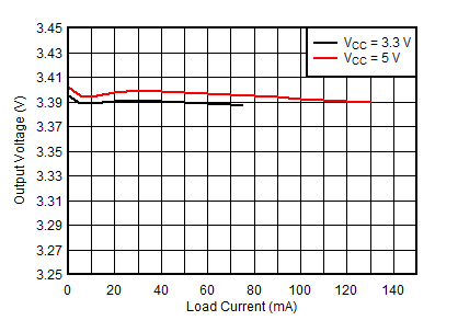
VISO = 3.3 V TA = 25°C
Figure 3. Isolated Supply Voltage (VISO) vs Load Current (IISO)
ISOW7821 D005_SLLSEY2.gif
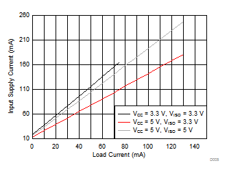
TA = 25°C
Figure 5. ISOW7821 Supply Current (ICC) vs Load Current (IISO)
ISOW7821 D007_SLLSEY2.gif
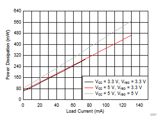
TA = 25°C
Figure 7. Power Dissipation vs Load Current (IISO)
ISOW7821 D009_SLLSEY2.gif
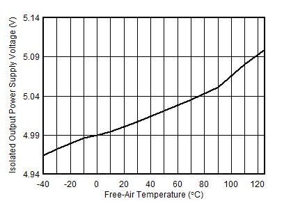
No IISO load VCC = 5 V VISO = 5 V
Figure 9. 5-V Isolated Supply Voltage (VISO) vs Free-Air Temperature
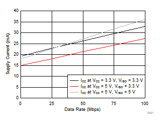
ISOW7821 D001.gif
CL = 15 pF TA = 25°C No IISO load
Figure 11. Supply Current vs Data Rate
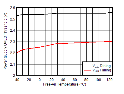
ISOW7821 D013_SLLSEY2.gif
Figure 13. Power-Supply Undervoltage Threshold vs Free Air Temperature
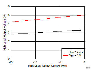
ISOW7821 D015_SLLSEY2.gif
TA = 25°C
Figure 15. High-Level Output Voltage vs High-Level Output Current
ISOW7821 isow784x-load-transient-response.gif
VCC = 5 V VISO = 3.3 V
1. Negligible undershoot and overshoot because of load transient
Figure 17. 10-mA to 110-mA Load Transient Response
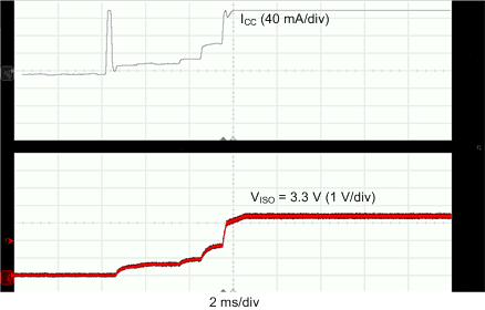
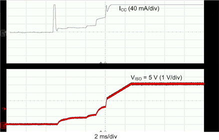
ISOW7821 isow784x-soft-start-120-ma-load.gif
VCC = 5 V VISO = 3.3 V
Input current spike is because of charging the input supply decoupling capacitor
Figure 19. Soft Start at 120-mA Load
ISOW7821 isow784x-soft-start-130-ma-load.gif
VCC = 5 V VISO = 5 V
Input current spike is because of charging the input supply decoupling capacitor
Figure 21. Soft Start at 130-mA Load
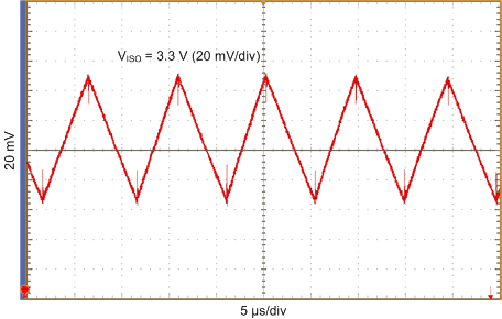
ISOW7821 isow784x-viso-ripple-voltage-130-ma-viso-3p3v.gif
VCC = 5 V VISO = 3.3 V
Figure 23. VISO Ripple Voltage at 130 mA
ISOW7821 D004_SLLSEY2.gif
VISO = 5 V TA = 25°C
Figure 4. Isolated Supply Voltage (VISO) vs Load Current (IISO)
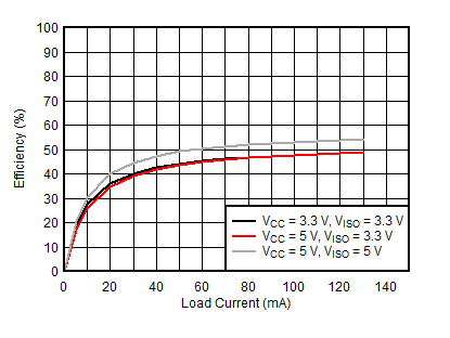
ISOW7821 D006_SLLSEY2.gif
TA = 25°C
Figure 6. Efficiency vs Load Current (IISO)
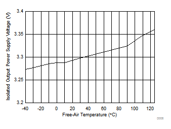
ISOW7821 D008_SLLSEY2.gif
No IISO load VCC = 5 V VISO = 3.3 V
Figure 8. 3.3-V Isolated Supply Voltage (VISO) vs Free-Air Temperature
ISOW7821 D010_SLLSEY2.gif
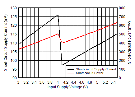
VISO shorted to GND2 TA = 25°C
Figure 10. Short-Circuit Supply Current (ICC) and Power (P) vs Supply Voltage (VCC)
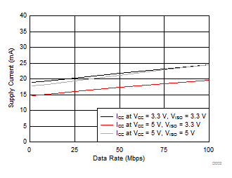
ISOW7821 D002.gif
CL = no load TA = 25°C No IISO load
Figure 12. Supply Current vs Data Rate
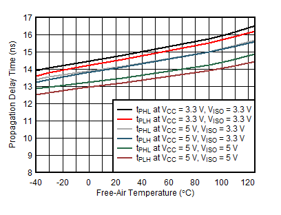
ISOW7821 D014_SLLSEY2.gif
Figure 14. Propagation Delay Time vs Free-Air Temperature
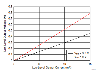
ISOW7821 D016_SLLSEY2.gif
TA = 25°C
Figure 16. Low-Level Output Voltage vs Low-Level Output Current
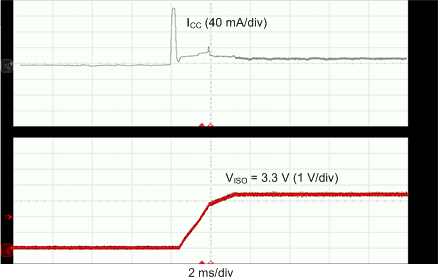
ISOW7821 isow784x-soft-start-10-ma-load-viso-3p3v.gif
VCC = 5 V VISO = 3.3 V
Current spike is because of charging the input supply capacitor
Figure 18. Soft Start at 10-mA Load
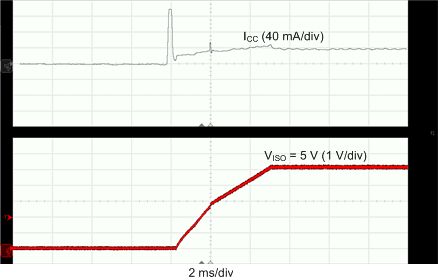
ISOW7821 isow784x-soft-start-10-ma-load-viso-5v.gif
VCC = 5 V VISO = 5 V
Input current spike is because of charging the input supply decoupling capacitor
Figure 20. Soft Start at 10-mA Load
ISOW7821 isow784x-viso-ripple-voltage-130-ma-viso-5v.gif
VCC = 5 V VISO = 5 V
Figure 22. VISO Ripple Voltage at 130 mA