JAJSE60B November 2017 – September 2019 ISOW7821
PRODUCTION DATA.
- 1 特長
- 2 アプリケーション
- 3 概要
- 4 改訂履歴
- 5 概要(続き)
- 6 Pin Configuration and Functions
-
7 Specifications
- 7.1 Absolute Maximum Ratings
- 7.2 ESD Ratings
- 7.3 Recommended Operating Conditions
- 7.4 Thermal Information
- 7.5 Power Ratings
- 7.6 Insulation Specifications
- 7.7 Safety-Related Certifications
- 7.8 Safety Limiting Values
- 7.9 Electrical Characteristics—5-V Input, 5-V Output
- 7.10 Supply Current Characteristics—5-V Input, 5-V Output
- 7.11 Electrical Characteristics—5-V Input, 3.3-V Output
- 7.12 Supply Current Characteristics—5-V Input, 3.3-V Output
- 7.13 Electrical Characteristics—3.3-V Input, 3.3-V Output
- 7.14 Supply Current Characteristics—3.3-V Input, 3.3-V Output
- 7.15 Switching Characteristics—5-V Input, 5-V Output
- 7.16 Switching Characteristics—5-V Input, 3.3-V Output
- 7.17 Switching Characteristics—3.3-V Input, 3.3-V Output
- 7.18 Insulation Characteristics Curves
- 7.19 Typical Characteristics
- 8 Parameter Measurement Information
- 9 Detailed Description
- 10Application and Implementation
- 11Power Supply Recommendations
- 12Layout
- 13デバイスおよびドキュメントのサポート
- 14メカニカル、パッケージ、および注文情報
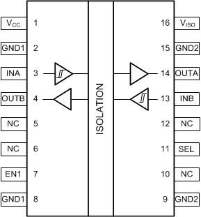
6 Pin Configuration and Functions
DWE Package
16-Pin SOIC-WB
Top View

Pin Functions
| PIN | I/O | DESCRIPTION | |
|---|---|---|---|
| NAME | NO. | ||
| EN1 | 7 | — | Output enable for side 1.
Output pins on side 1 are enabled when EN1 is high or open. Output pins on side 1 are high impedance when EN1 is low. |
| GND1 | 2, 8 | — | Ground connection for VCC |
| GND2 | 9, 15 | — | Ground connection for VISO |
| INA | 3 | I | Input channel A |
| OUTB | 4 | I | Output channel B |
| NC | 5 | — | Not connected |
| NC | 6 | — | Not connected |
| NC | 10 | — | Not connected |
| NC | 12 | — | Not connected |
| OUTA | 14 | O | Output channel A |
| INB | 13 | O | Input channel B |
| SEL | 11 | I | VISO selection pin.
VISO = 5 V when SEL is connected to VISO. VISO = 3.3 V, when SEL is connected to GND2 or left floating. For more information see the Device Functional Modes. |
| VCC | 1 | — | Supply voltage |
| VISO | 16 | — | Isolated supply voltage determined by SEL pin |