JAJSE60B November 2017 – September 2019 ISOW7821
PRODUCTION DATA.
- 1 特長
- 2 アプリケーション
- 3 概要
- 4 改訂履歴
- 5 概要(続き)
- 6 Pin Configuration and Functions
-
7 Specifications
- 7.1 Absolute Maximum Ratings
- 7.2 ESD Ratings
- 7.3 Recommended Operating Conditions
- 7.4 Thermal Information
- 7.5 Power Ratings
- 7.6 Insulation Specifications
- 7.7 Safety-Related Certifications
- 7.8 Safety Limiting Values
- 7.9 Electrical Characteristics—5-V Input, 5-V Output
- 7.10 Supply Current Characteristics—5-V Input, 5-V Output
- 7.11 Electrical Characteristics—5-V Input, 3.3-V Output
- 7.12 Supply Current Characteristics—5-V Input, 3.3-V Output
- 7.13 Electrical Characteristics—3.3-V Input, 3.3-V Output
- 7.14 Supply Current Characteristics—3.3-V Input, 3.3-V Output
- 7.15 Switching Characteristics—5-V Input, 5-V Output
- 7.16 Switching Characteristics—5-V Input, 3.3-V Output
- 7.17 Switching Characteristics—3.3-V Input, 3.3-V Output
- 7.18 Insulation Characteristics Curves
- 7.19 Typical Characteristics
- 8 Parameter Measurement Information
- 9 Detailed Description
- 10Application and Implementation
- 11Power Supply Recommendations
- 12Layout
- 13デバイスおよびドキュメントのサポート
- 14メカニカル、パッケージ、および注文情報
10.2.3.1 Insulation Lifetime
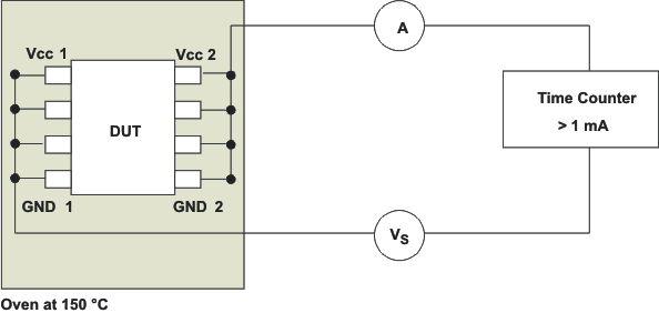
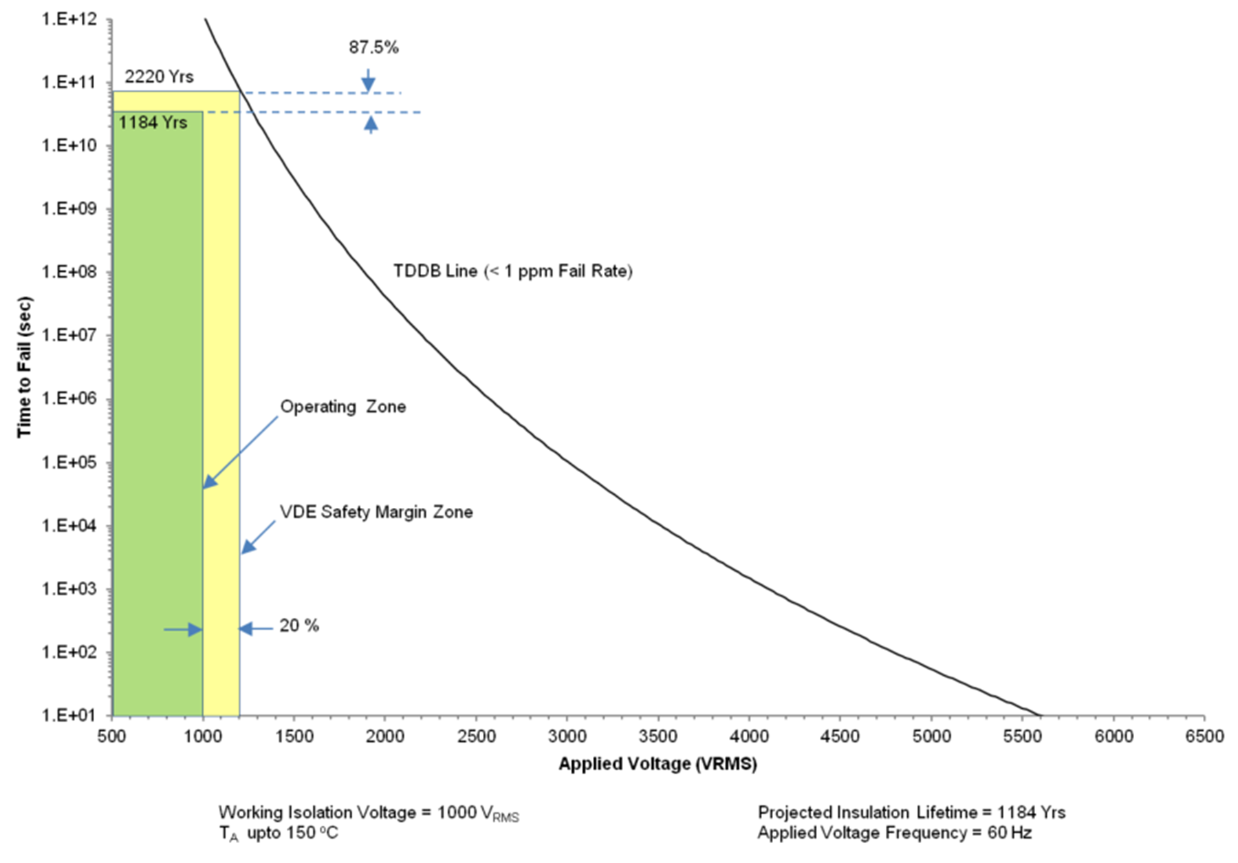
Insulation lifetime projection data is collected by using industry-standard Time Dependent Dielectric Breakdown (TDDB) test method. In this test, all pins on each side of the barrier are tied together creating a two-terminal device and high voltage applied between the two sides; See Figure 33 for TDDB test setup. The insulation breakdown data is collected at various high voltages switching at 60 Hz over temperature. For reinforced insulation, VDE standard requires the use of TDDB projection line with failure rate of less than 1 part per million (ppm). Even though the expected minimum insulation lifetime is 20 years at the specified working isolation voltage, VDE reinforced certification requires additional safety margin of 20% for working voltage and 87.5% for lifetime which translates into minimum required insulation lifetime of 37.5 years at a working voltage that's 20% higher than the specified value.
Figure 34 shows the intrinsic capability of the isolation barrier to withstand high voltage stress over its lifetime. Based on the TDDB data, the intrinsic capability of the insulation is 1000 VRMS with a lifetime of 1184 years.
 Figure 33. Test Setup for Insulation Lifetime Measurement
  Figure 34. Insulation Lifetime Projection Data