JAJS558H september 1998 – june 2023 LM2676
PRODUCTION DATA
- 1
- 1 特長
- 2 アプリケーション
- 3 概要
- 4 Revision History
- 5 概要 (続き)
- 6 Pin Configuration and Functions
-
7 Specifications
- 7.1 Absolute Maximum Ratings
- 7.2 ESD Ratings
- 7.3 Recommended Operating Conditions
- 7.4 Thermal Information
- 7.5 Electrical Characteristics – 3.3-V Version
- 7.6 Electrical Characteristics – 5-V Version
- 7.7 Electrical Characteristics – 12-V Version
- 7.8 Electrical Characteristics – Adjustable Voltage Version
- 7.9 Electrical Characteristics – All Output Voltage Versions
- 7.10 Typical Characteristics
- 8 Detailed Description
-
9 Application and Implementation
- 9.1 Application Information
- 9.2
Typical Applications
- 9.2.1 Fixed Output Voltage Typical Application
- 9.2.2 Adjustable Output Voltage Typical Application
- 9.2.3 Typical Application for All Output Voltage Versions
- 9.3 Power Supply Recommendations
- 9.4 Layout
- 10Device and Documentation Support
- 11Mechanical, Packaging, and Orderable Information
パッケージ・オプション
メカニカル・データ(パッケージ|ピン)
サーマルパッド・メカニカル・データ
発注情報
9.2.2 Adjustable Output Voltage Typical Application

CIN =
22-μF, 50-V Tantalum, Sprague 199D Series
COUT = 47-μF, 25-V Tantalum, Sprague 595D Series
D1 = 3.3-A, 50-V Schottky Rectifier, IR 30WQ05F
L1 = 68-μH Sumida #RCR110D-680L
R1 = 1.5 kΩ, 1%
CB = 0.01-μF, 50-V Ceramic
For a 5-V output, select R2 to be 4.75 kΩ, 1%
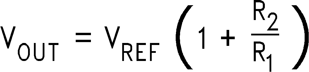
where VREF = 1.21 V
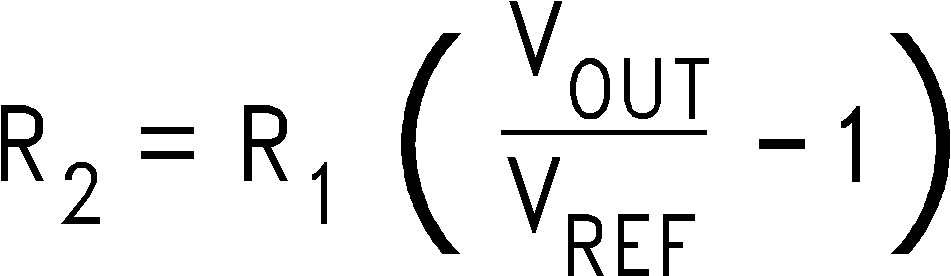
Use a 1% resistor for best stability.
Figure 9-5 Adjustable Output Voltage
VersionCOUT = 47-μF, 25-V Tantalum, Sprague 595D Series
D1 = 3.3-A, 50-V Schottky Rectifier, IR 30WQ05F
L1 = 68-μH Sumida #RCR110D-680L
R1 = 1.5 kΩ, 1%
CB = 0.01-μF, 50-V Ceramic
For a 5-V output, select R2 to be 4.75 kΩ, 1%
where VREF = 1.21 V
Use a 1% resistor for best stability.