JAJS558H september   1998  – june 2023 LM2676

PRODUCTION DATA  

  1.   1
  2. 特長
  3. アプリケーション
  4. 概要
  5. Revision History
  6. 概要 (続き)
  7. Pin Configuration and Functions
  8. Specifications
    1. 7.1  Absolute Maximum Ratings
    2. 7.2  ESD Ratings
    3. 7.3  Recommended Operating Conditions
    4. 7.4  Thermal Information
    5. 7.5  Electrical Characteristics – 3.3-V Version
    6. 7.6  Electrical Characteristics – 5-V Version
    7. 7.7  Electrical Characteristics – 12-V Version
    8. 7.8  Electrical Characteristics – Adjustable Voltage Version
    9. 7.9  Electrical Characteristics – All Output Voltage Versions
    10. 7.10 Typical Characteristics
  9. Detailed Description
    1. 8.1 Overview
    2. 8.2 Functional Block Diagram
    3. 8.3 Feature Description
      1. 8.3.1 Adjustable Output Voltage
    4. 8.4 Device Functional Modes
      1. 8.4.1 Shutdown Mode
      2. 8.4.2 Active Mode
  10. Application and Implementation
    1. 9.1 Application Information
    2. 9.2 Typical Applications
      1. 9.2.1 Fixed Output Voltage Typical Application
        1. 9.2.1.1 Design Requirements
        2. 9.2.1.2 Detailed Design Procedure
          1. 9.2.1.2.1 Custom Design with WEBENCH® Tools
          2. 9.2.1.2.2 Inductor Selection (L1)
          3. 9.2.1.2.3 Output Capacitor Selection (COUT)
          4. 9.2.1.2.4 Catch Diode Selection (D1)
          5. 9.2.1.2.5 Input Capacitor (CIN)
          6. 9.2.1.2.6 Boost Capacitor (CB)
        3. 9.2.1.3 Application Curves
      2. 9.2.2 Adjustable Output Voltage Typical Application
        1. 9.2.2.1 Design Requirements
        2. 9.2.2.2 Detailed Design Procedure
          1. 9.2.2.2.1 Programming Output Voltage
          2. 9.2.2.2.2 Inductor Selection (L1)
          3. 9.2.2.2.3 Output Capacitor Selection (COUT)
          4. 9.2.2.2.4 Catch Diode Selection (D1)
          5. 9.2.2.2.5 Input Capacitor (CIN)
          6. 9.2.2.2.6 Boost Capacitor (CB)
        3. 9.2.2.3 Application Curves
      3. 9.2.3 Typical Application for All Output Voltage Versions
        1. 9.2.3.1 Application Curves
    3. 9.3 Power Supply Recommendations
    4. 9.4 Layout
      1. 9.4.1 Layout Guidelines
        1. 9.4.1.1 WSON Package Devices
      2. 9.4.2 Layout Examples
  11. 10Device and Documentation Support
    1. 10.1 Device Support
      1. 10.1.1 Development Support
        1. 10.1.1.1 Custom Design with WEBENCH® Tools
    2. 10.2 Documentation Support
      1. 10.2.1 Related Documentation
    3. 10.3 ドキュメントの更新通知を受け取る方法
    4. 10.4 サポート・リソース
    5. 10.5 Trademarks
    6. 10.6 静電気放電に関する注意事項
    7. 10.7 用語集
  12. 11Mechanical, Packaging, and Orderable Information

パッケージ・オプション

メカニカル・データ(パッケージ|ピン)
サーマルパッド・メカニカル・データ
発注情報

Application Curves

GUID-1228C6D7-8079-45FE-B71C-20A676C431C2-low.png
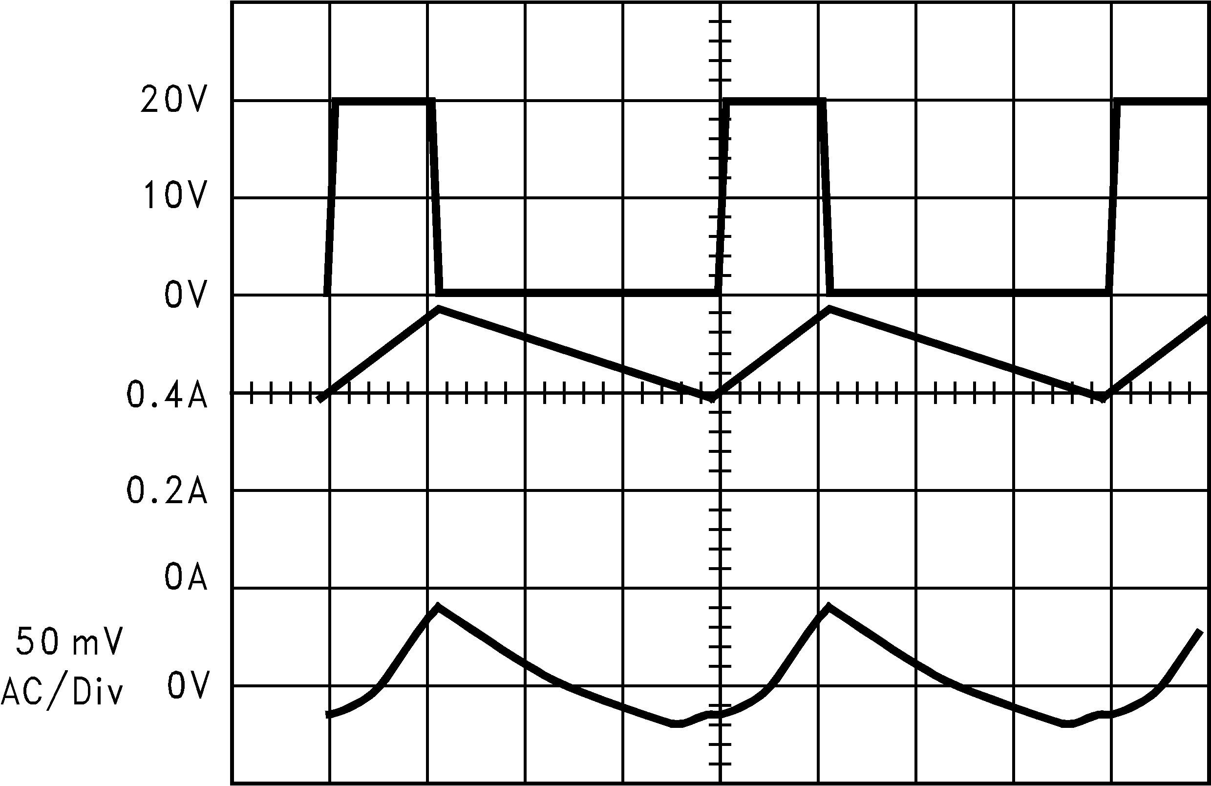
Continuous mode switching waveforms VIN = 20 V, VOUT = 5 V, ILOAD = 500 mA L = 100 μH, COUT = 100 μF, COUTESR = 0.1 Ω
A: VSW pin voltage = 10 V/div
B: Inductor current = 0.2 A/div
C: Output ripple voltage = 50 mV/div ac-coupled
Figure 9-3 Horizontal Time Base: 1 μs/div
GUID-9B3B2C32-08E8-42F6-BA4C-DEC82C656BA8-low.png
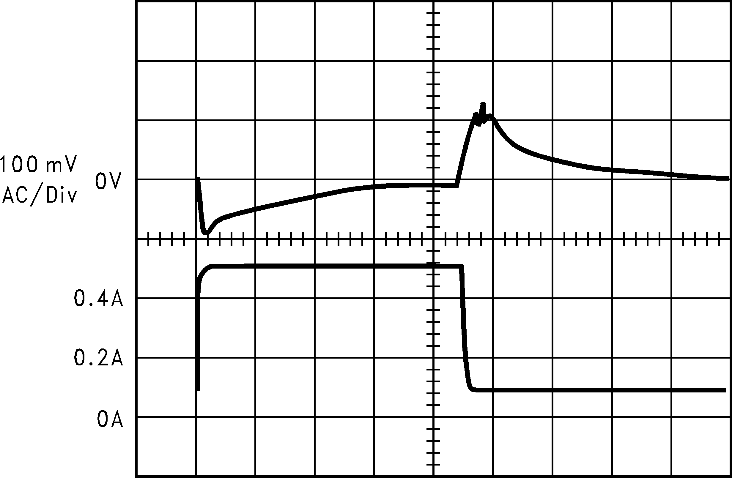
Load transient response for continuous mode VIN = 20 V, VOUT = 5 V, L = 100 μH, COUT = 100 μF, COUTESR = 0.1 Ω
A: Output voltage = 100 mV/div, ac-coupled
B: Load current = 100-mA to 500-mA load pulse
Figure 9-4 Horizontal Time Base: 50 μs/div