JAJS558H september 1998 – june 2023 LM2676
PRODUCTION DATA
- 1
- 1 特長
- 2 アプリケーション
- 3 概要
- 4 Revision History
- 5 概要 (続き)
- 6 Pin Configuration and Functions
-
7 Specifications
- 7.1 Absolute Maximum Ratings
- 7.2 ESD Ratings
- 7.3 Recommended Operating Conditions
- 7.4 Thermal Information
- 7.5 Electrical Characteristics – 3.3-V Version
- 7.6 Electrical Characteristics – 5-V Version
- 7.7 Electrical Characteristics – 12-V Version
- 7.8 Electrical Characteristics – Adjustable Voltage Version
- 7.9 Electrical Characteristics – All Output Voltage Versions
- 7.10 Typical Characteristics
- 8 Detailed Description
-
9 Application and Implementation
- 9.1 Application Information
- 9.2
Typical Applications
- 9.2.1 Fixed Output Voltage Typical Application
- 9.2.2 Adjustable Output Voltage Typical Application
- 9.2.3 Typical Application for All Output Voltage Versions
- 9.3 Power Supply Recommendations
- 9.4 Layout
- 10Device and Documentation Support
- 11Mechanical, Packaging, and Orderable Information
パッケージ・オプション
メカニカル・データ(パッケージ|ピン)
サーマルパッド・メカニカル・データ
発注情報
9.2.2.2.1 Programming Output Voltage
Select R1 and R2, as shown in Figure 9-5.
Use the following formula to select the appropriate resistor values.
Equation 1. 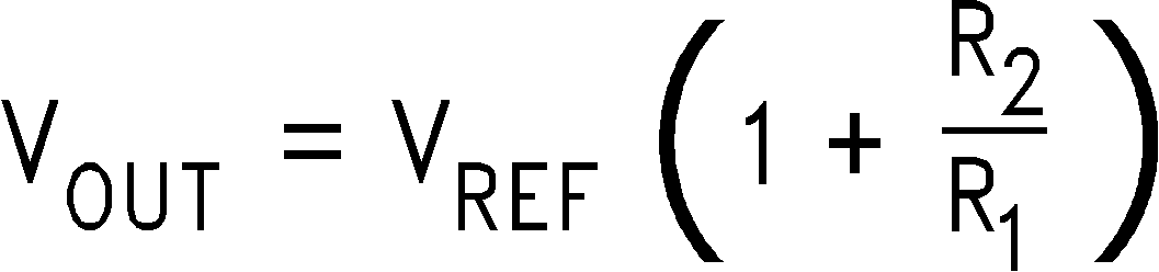
where
- VREF = 1.21 V
Select a value for R1 between 240 Ω and 1.5 kΩ. The lower resistor values minimize noise pickup in the sensitive feedback pin. (For the lowest temperature coefficient and the best stability with time, use 1% metal film resistors.)
Equation 2. 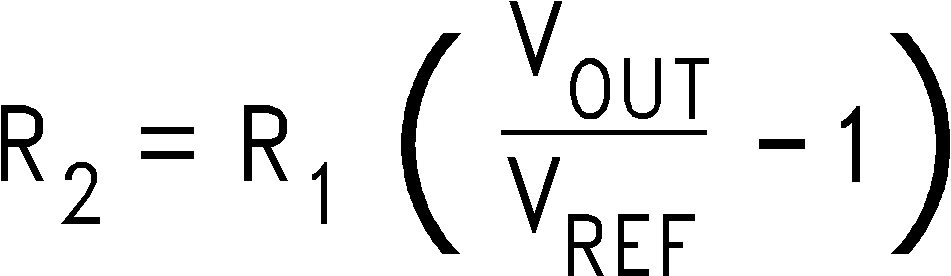
Select R1 to be 1 kΩ, 1%. Solve for R2.
Equation 3. 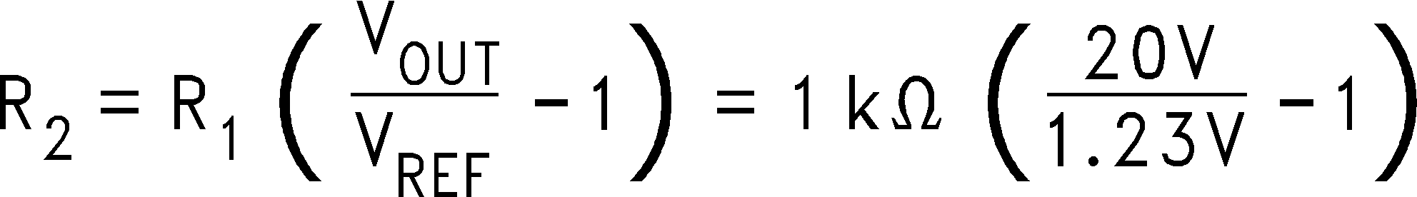
where
- R2 = 1k (16.53 − 1) = 15.53 kΩ, closest 1% value is 15.4 kΩ
R2 = 15.4 kΩ