SLVSES8A October 2020 – December 2020 LM5127-Q1
PRODUCTION DATA
- 1 Features
- 2 Applications
- 3 Description
- 4 Revision History
- 5 Description (continued)
- 6 Pin Configuration and Functions
- 7 Specifications
-
8 Detailed Description
- 8.1 Overview
- 8.2 Functional Block Diagram
- 8.3
Feature Description
- 8.3.1 Device Enable (EN, VCC_HOLD)
- 8.3.2 Dual Input VCC Regulator (BIAS, VCCX, VCC)
- 8.3.3 Dual Input VDD Switch (VDD, VDDX)
- 8.3.4 Device Configuration and Light Load Switching Mode Selection (CFG/MODE)
- 8.3.5 Fixed or Adjustable Output Regulation Target (VOUT, FB)
- 8.3.6 Overvoltage Protection (VOUT, FB)
- 8.3.7 Power Good Indicator (PGOOD)
- 8.3.8 Programmable Switching Frequency (RT)
- 8.3.9 External Clock Synchronization (SYNC)
- 8.3.10 Programmable Spread Spectrum (DITHER)
- 8.3.11 Programmable Soft Start (SS)
- 8.3.12 Fast Re-start using VCC_HOLD (VCC_HOLD)
- 8.3.13 Transconductance Error Amplifier and PWM (COMP)
- 8.3.14 Current Sensing and Slope Compensation (CSA, CSB)
- 8.3.15 Constant Peak Current Limit (CSA, CSB)
- 8.3.16 Maximum Duty Cycle and Minimum Controllable On-time Limits (Boost)
- 8.3.17 Bypass Mode (Boost)
- 8.3.18 Minimum Controllable On-time and Minimum Controllable Off-time Limits (Buck)
- 8.3.19 Low Dropout Mode for Extended Minimum Input Voltage (Buck)
- 8.3.20 Programmable Hiccup Mode Overload Protection (RES)
- 8.3.21 MOSFET Drivers and Hiccup Mode Fault Protection (LO, HO, HB)
- 8.3.22 Battery Monitor (BMOUT, BMIN_FIX, BMIN_PRG)
- 8.3.23 Dual-phase Interleaved Configuration for High Current Supply (CFG)
- 8.3.24 Thermal Shutdown Protection
- 8.3.25 External VCCX Supply Reduces Power Dissipation
- 8.4 Device Functional Modes
- 9 Application and Implementation
- 10Power Supply Recommendations
- 11Layout
- 12Device and Documentation Support
- 13Mechanical, Packaging, and Orderable Information
パッケージ・オプション
メカニカル・データ(パッケージ|ピン)
- RGZ|48
サーマルパッド・メカニカル・データ
- RGZ|48
発注情報
8.3.18 Minimum Controllable On-time and Minimum Controllable Off-time Limits (Buck)
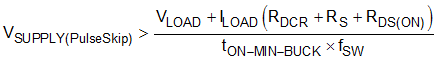
In buck configuration, the device starts pulse skipping at the light load condition or when the input voltage is much higher than the target output voltage in CCM. The device skips the high-side driver pulses if the required on-time is less than the buck minimum controllable on-time (tON-MIN-BUCK). This pulse skipping appears as a random behavior.
If the input supply voltage satisfies the following inequality in CCM, the buck channel starts random pulse skipping.
| 3.3-V OUTPUT | 5.0-V OUTPUT | |
|---|---|---|
| fSW = 440 kHz | No pulse skipping in CCM | No pulse skipping in CCM |
| fSW = 2.2 MHz | > 20 - 23 V | > 31 - 34 V |
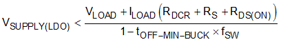
In buck configuration, the maximum duty cycle of the high-side driver is limited by the buck minimum controllable off-time (tOFF-MIN-BUCK). tOFF-MIN-BUCK decides the minimum input supply voltage that can achieve the target output voltage in normal PWM operation. If the input voltage falls down below this minimum input supply voltage in normal PWM operation, the device enters a low-dropout (LDO) mode to extend the minimum input voltage further down. If the input supply voltage satisfies the following inequality, the buck channel enters a low drop-out mode.
| 3.3-V OUTPUT | 5.0-V OUTPUT | |
|---|---|---|
| fSW = 440 kHz | < 3.6 - 3.8 V | < 5.5 - 5.6 V |
| fSW = 2.2 MHz | < 4.3 - 4.5 V | < 6.6 - 6.7 V |