SLVSES8A October 2020 – December 2020 LM5127-Q1
PRODUCTION DATA
- 1 Features
- 2 Applications
- 3 Description
- 4 Revision History
- 5 Description (continued)
- 6 Pin Configuration and Functions
- 7 Specifications
-
8 Detailed Description
- 8.1 Overview
- 8.2 Functional Block Diagram
- 8.3
Feature Description
- 8.3.1 Device Enable (EN, VCC_HOLD)
- 8.3.2 Dual Input VCC Regulator (BIAS, VCCX, VCC)
- 8.3.3 Dual Input VDD Switch (VDD, VDDX)
- 8.3.4 Device Configuration and Light Load Switching Mode Selection (CFG/MODE)
- 8.3.5 Fixed or Adjustable Output Regulation Target (VOUT, FB)
- 8.3.6 Overvoltage Protection (VOUT, FB)
- 8.3.7 Power Good Indicator (PGOOD)
- 8.3.8 Programmable Switching Frequency (RT)
- 8.3.9 External Clock Synchronization (SYNC)
- 8.3.10 Programmable Spread Spectrum (DITHER)
- 8.3.11 Programmable Soft Start (SS)
- 8.3.12 Fast Re-start using VCC_HOLD (VCC_HOLD)
- 8.3.13 Transconductance Error Amplifier and PWM (COMP)
- 8.3.14 Current Sensing and Slope Compensation (CSA, CSB)
- 8.3.15 Constant Peak Current Limit (CSA, CSB)
- 8.3.16 Maximum Duty Cycle and Minimum Controllable On-time Limits (Boost)
- 8.3.17 Bypass Mode (Boost)
- 8.3.18 Minimum Controllable On-time and Minimum Controllable Off-time Limits (Buck)
- 8.3.19 Low Dropout Mode for Extended Minimum Input Voltage (Buck)
- 8.3.20 Programmable Hiccup Mode Overload Protection (RES)
- 8.3.21 MOSFET Drivers and Hiccup Mode Fault Protection (LO, HO, HB)
- 8.3.22 Battery Monitor (BMOUT, BMIN_FIX, BMIN_PRG)
- 8.3.23 Dual-phase Interleaved Configuration for High Current Supply (CFG)
- 8.3.24 Thermal Shutdown Protection
- 8.3.25 External VCCX Supply Reduces Power Dissipation
- 8.4 Device Functional Modes
- 9 Application and Implementation
- 10Power Supply Recommendations
- 11Layout
- 12Device and Documentation Support
- 13Mechanical, Packaging, and Orderable Information
パッケージ・オプション
メカニカル・データ(パッケージ|ピン)
- RGZ|48
サーマルパッド・メカニカル・データ
- RGZ|48
発注情報
9.2.2.2 Application Ideas
For applications requiring the lowest cost with minimum conduction loss, inductor DC resistance (DCR) can be used to sense the inductor current rather than using a sense resistor. RDCRC and CDCRC must meet Equation 23 to match the time constant.
 Buck, (b)
Boost") Figure 9-2 DCR Current Sensing (a) Buck, (b)
Boost
Figure 9-2 DCR Current Sensing (a) Buck, (b)
Boost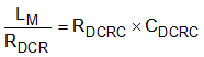
When CH1 is used as a pre-boost, the output undershoot during a cold-cranking event can be minimized by adding an R-C in parallel with the low-side feedback resistor. A lower value of ROS will result in a lower output undershoot (see Figure 9-3). The COS value should be large enough not to affect loop response in normal operation. Use 20-kΩ and 4.7-nF combination as a starting point and then adjust the values if required.
 Figure 9-3 VOUT Boost Circuit
The light load switching mode can be dynamically programmed during operation between FPWM and DE mode.
 Figure 9-4 Dynamic Transition Between FPWM and DE
If required, an additional PGOOD or BMOUT delay can be programmed using an external circuit.
 Figure 9-5 Additional PGOOD / BMOUT Delay
Sequential start-up can be realized by using the PGOOD pins.
 Figure 9-6 Sequential Start-up
Switching can be stopped individually by pulling down the SS pins.
 Figure 9-7 Stop Switching using SS Pin