SLVSES8A October 2020 – December 2020 LM5127-Q1
PRODUCTION DATA
- 1 Features
- 2 Applications
- 3 Description
- 4 Revision History
- 5 Description (continued)
- 6 Pin Configuration and Functions
- 7 Specifications
-
8 Detailed Description
- 8.1 Overview
- 8.2 Functional Block Diagram
- 8.3
Feature Description
- 8.3.1 Device Enable (EN, VCC_HOLD)
- 8.3.2 Dual Input VCC Regulator (BIAS, VCCX, VCC)
- 8.3.3 Dual Input VDD Switch (VDD, VDDX)
- 8.3.4 Device Configuration and Light Load Switching Mode Selection (CFG/MODE)
- 8.3.5 Fixed or Adjustable Output Regulation Target (VOUT, FB)
- 8.3.6 Overvoltage Protection (VOUT, FB)
- 8.3.7 Power Good Indicator (PGOOD)
- 8.3.8 Programmable Switching Frequency (RT)
- 8.3.9 External Clock Synchronization (SYNC)
- 8.3.10 Programmable Spread Spectrum (DITHER)
- 8.3.11 Programmable Soft Start (SS)
- 8.3.12 Fast Re-start using VCC_HOLD (VCC_HOLD)
- 8.3.13 Transconductance Error Amplifier and PWM (COMP)
- 8.3.14 Current Sensing and Slope Compensation (CSA, CSB)
- 8.3.15 Constant Peak Current Limit (CSA, CSB)
- 8.3.16 Maximum Duty Cycle and Minimum Controllable On-time Limits (Boost)
- 8.3.17 Bypass Mode (Boost)
- 8.3.18 Minimum Controllable On-time and Minimum Controllable Off-time Limits (Buck)
- 8.3.19 Low Dropout Mode for Extended Minimum Input Voltage (Buck)
- 8.3.20 Programmable Hiccup Mode Overload Protection (RES)
- 8.3.21 MOSFET Drivers and Hiccup Mode Fault Protection (LO, HO, HB)
- 8.3.22 Battery Monitor (BMOUT, BMIN_FIX, BMIN_PRG)
- 8.3.23 Dual-phase Interleaved Configuration for High Current Supply (CFG)
- 8.3.24 Thermal Shutdown Protection
- 8.3.25 External VCCX Supply Reduces Power Dissipation
- 8.4 Device Functional Modes
- 9 Application and Implementation
- 10Power Supply Recommendations
- 11Layout
- 12Device and Documentation Support
- 13Mechanical, Packaging, and Orderable Information
パッケージ・オプション
メカニカル・データ(パッケージ|ピン)
- RGZ|48
サーマルパッド・メカニカル・データ
- RGZ|48
発注情報
8.3.15 Constant Peak Current Limit (CSA, CSB)
In boost configuration, if the current sense amplifier input exceeds the 60-mV cycle-by-cycle current limit threshold (VCLTH), the current limit comparator immediately terminates LO and turns on HO. In buck configuration, if the current sense amplifier input exceeds VCLTH, the current limit comparator immediately terminates HO and turns on LO.
The device provides a constant peak current limit whose peak inductor current limit is constant over the input and output voltage. For the case where the inductor current may overshoot, such as inductor saturation, the current limit comparator skips pulses until the current has decayed below the current limit threshold.
 Figure 8-14 Current Limit Comparator
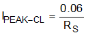
Cycle-by-cycle peak current limit is calculated as follows:
 PWM
Comparator Input") Figure 8-15 (a) PWM
Comparator Input
Figure 8-15 (a) PWM
Comparator Input Current Limit Comparator Input (Buck and
Boost)") Figure 8-16 (b) Current Limit Comparator Input (Buck and
Boost)
Figure 8-16 (b) Current Limit Comparator Input (Buck and
Boost)Boost converters have a natural pass-through path from the supply to the load through the high-side MOSFET body diode. Due to the pass-through path and the limitation of the minimum controllable on-time, boost converters cannot provide current limit protection when the output voltage is close to or less than the input supply voltage.