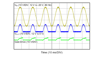
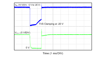
SNOSCZ1B July 2015 – June 2016 LM74610-Q1
PRODUCTION DATA.
- 1 Features
- 2 Applications
- 3 Description
- 4 Revision History
- 5 Pin Configuration and Functions
- 6 Specifications
- 7 Detailed Description
- 8 Application and Implementation
- 9 Power Supply Recommendations
- 10Layout
- 11Device and Documentation Support
- 12Mechanical, Packaging, and Orderable Information
8 Application and Implementation
NOTE
Information in the following applications sections is not part of the TI component specification, and TI does not warrant its accuracy or completeness. TI’s customers are responsible for determining suitability of components for their purposes. Customers should validate and test their design implementation to confirm system functionality.
8.1 Application Information
The LM74610-Q1 is used with N-Channel MOSFET controller in a typical reverse polarity protection application. This device is connected to the N-Channel MOSFET as shown in Figure 12 . The schematic for the typical application is shown in Figure 13 where the LM74610-Q1 is used in series with a battery to drive the MOSFET Q1. The TVS+ and TVS- are not required for the LM74610-Q1. However, they are typically used to clamp the positive and negative voltage surges respectively. The output capacitor Cout is recommended to protect the immediate output voltage collapse as a result of line disturbance.
8.2 Typical Application
 Figure 12. Typical System Application
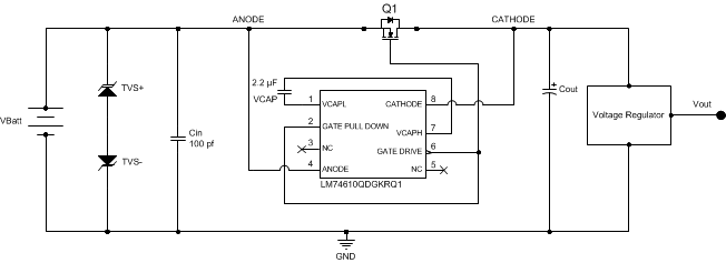 Figure 13. Typical Application Schematic
8.2.1 Design Requirements
For this design example, use the parameters listed in Table 1 as the input parameters
Table 1. Design Parameters
| DESIGN PARAMETER | EXAMPLE VALUE |
|---|---|
| Input voltage range | Max VDS of the MOSFET |
| Output Voltage | Max VDS of the MOSFET |
| Maximum Negative Voltage | -45V |
| Output Current Range | Maximum drain current |
| Output Capacitance | 47µF |
| Transient Response, 3A Load Step | ΔVo = ± 5% |
8.2.2 Detailed Design Procedure
To begin the design process, determine the following:
8.2.2.1 Design Considerations
- Input voltage range
- Output current range
- Body Diode forward voltage drop for the selected MOSFET
- MOSFET Gate threshold voltage
8.2.2.2 Startup Voltage
The LM74610-Q1 will not initiate the charge pump operation if a closed loop system is in standby mode or the drain current is smaller than 1mA (typical). This is due to a minimum body diode voltage requirement of the LM74610-Q1 controller. If the drain current is too small to produce a minimum voltage drop of 0.48V at 25 ͦ C, the charge pump circuitry will remain off and the MOSFET will act just like a diode. It is very important to know the body diode voltage parameter of a MOSFET before implementing it into the Smart Diode solution. Some N-channels MOSFETs have very low body diode voltage at higher temperature. This makes their drain current requirement higher to achieve 0.48V across the body diode in order to initiate the LM74610-Q1 controller at higher temperatures.
8.2.2.3 Capacitor Selection
A ceramic capacitor should be placed between VcapL and VcapH. The capacitor acts as a holding tank to power up the control circuitry when the MOSFET is on.
When the MOSFET is off, this capacitor is charged up to higher voltage threshold of ~6.3 V. Once this voltage is reached, the Gate Drive of LM74610-Q1 will provide drive for the external MOSFET. When the MOSFET is ON, the voltage across its body diode is collapsed because the forward conduction is through the MOSFET. During this time, the capacitor acts as a supply for the Gate Drive to keep the MOSFET ON.
The capacitor voltage will gradually decay when the MOSFET is ON. Once the capacitor voltage reaches a lower voltage threshold of 5.15V, the MOSFET is turned off and the capacitor gets recharged again for the next cycle.
A capacitor value of 220nF to 4.7uF with X7R/COG characteristic and 16V rating or higher is recommended for this application. A higher value capacitor sets longer MOSFET ON time and OFF time; however, the duty cycle remains at ~98% for MOSFET ON time irrespective of capacitor value.
If the Vcap value is 2.2µF, the MOSFET ON time and OFF time can be calculated using Equation 1 :
The duty cycle can be calculated using Equation 5 :
8.2.2.4 MOSFET Selection
The LM74610-Q1 can provide up to 5V of gate to source voltage (VGS). The important MOSFET electrical parameters are the maximum continuous Drain current ID, the maximum drain-to-source voltage VDS(MAX), and the drain-to-source On resistance RDSON. The maximum continuous drain current, ID, rating must exceed the maximum continuous load current. The rating for the maximum current through the body diode, IS, is typically rated the same as, or slightly higher than the drain current, but body diode current only flows for a small period when the charge pump capacitor is being charged.
The voltage across the MOSFET's body diode must be higher than 0.48 V at low current. The body diode voltage for a MOFET typically decreases as the ambient temperature increases. This will increase the source current requirement to achieve the minimum body diode drain-to-source voltage for the charge pump to initiate. The maximum drain-to-source voltage, VDS(MAX), must be high enough to withstand the highest differential voltage seen in the application. This would include any anticipated fault conditions. The LM74610-Q1 does not have positive voltage limitation, however, it is recommended to use MOSFETs with voltage rating up to 45 V for automotive applications. Table 2 shows the examples of recommended MOSFETs to be used with the LM74610-Q1.
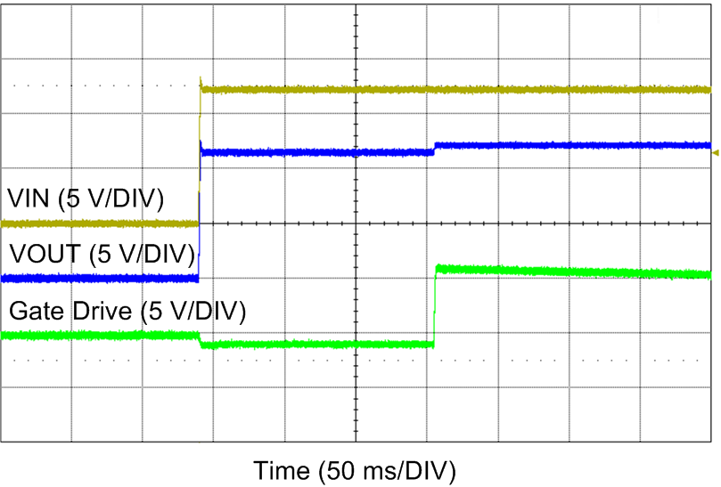
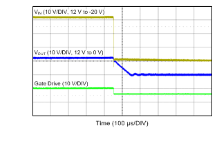
8.2.3 Application Curves
8.2.4 Selection of TVS Diodes in Automotive Reverse Polarity Applications
TVS diodes can be used in automotive systems for protection against transients. There are 2 types of TVS diode, one that offers bi-directional clamping and one that is uni-directional. In the application circuit show in Figure 12, 2 unidirectional TVS diodes are used. TVS + does the clamping for positive pulses as seen in load dump and TVS- does the clamping for negative pulses such as seen in the ISO specs.
There are two important specs to be aware of: breakdown voltage and clamping voltage. Breakdown voltage is the voltage at which the TVS diode goes into avalanche similar to a zener diode and is specified at a low current value typ 1mA. Clamping voltage is the voltage the TVS diode clamps to in high current pulse situations.
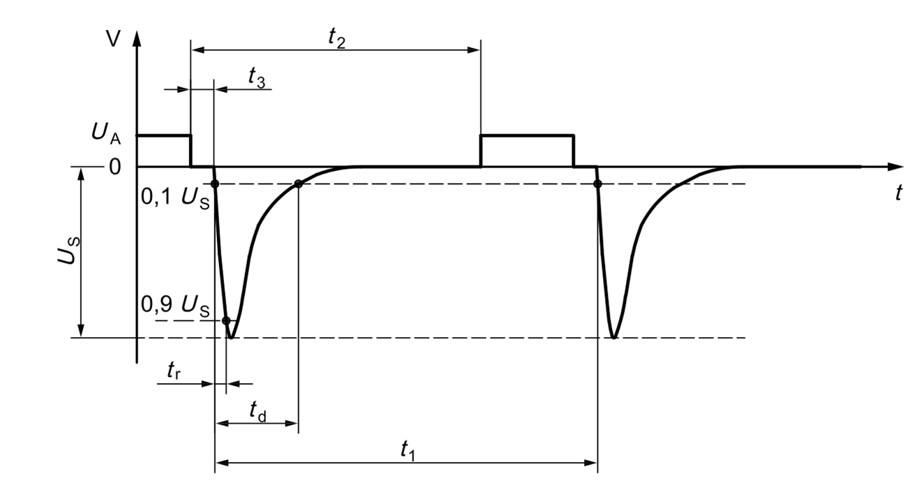
In the case of an ISO 7637-2 pulse 1, the voltages go to -150V with a generator impedance of 10Ω. This translates to 15A flowing through the TVS - and the voltage across the TVS would be close to its clamping voltage. A rule of thumb with TVS diode voltage selection is that the breakdown voltage should be higher than worst case steady state voltages seen in the system. TVS diodes are meant to clamp pulses and not meant for steady state voltages.
The value of the TVS + is selected such that the breakdown voltage of the TVS is higher than 24V which is a commonly used battery for jump start. LM74610-Q1 does not have a positive voltage limit so the selection of the voltage rating of TVS + is determined by the max voltage tolerated by the downstream electronics. If the downstream parts can withstand at least 37V (suppressed load dump) then there is no need to use the TVS+. In this case it can be replaced with a diode as seen in Figure 20. A 1A diode with a 30A surge current rating and at least 40V reverse voltage rating is recommended. In case positive clamping voltage is desired then SMBJ24A/SMBJ26A is recommended for TVS + as seen in Figure 12.
 Figure 20. Typical Application without Positive Voltage Clamping
The value of the TVS – is selected such that 2 criteria are met. The breakdown voltage of the TVS should be higher than the max reverse battery voltage which is typically 15V. The second criterion is that the abs max rating for reverse voltage of the LM74610 is not exceeded (-45V).
In case of reverse voltage pulses such as in ISO specs, the LM74610 turns the MOSFET off. When the MOSFET turns off the voltage seen by the LM74610, Anode to Cathode is - (clamping voltage of TVS- (plus) the output capacitor voltage). If the max voltage on output capacitors is 16V, then the clamping voltage of the TVS- should not exceed, 45V – 16V = 29V.
SMBJ14A/SMBJ15A/SMBJ16A TVS diodes can be used for TVS-. The breakdown voltage of SMBJ14A is 15.6V and SMBJ16A is 17.8V. This meets criteria one. The clamping voltage of SMBJ14A is 23.2V and SMBJ16A is 26V. This meets the second criteria.
Bi-directional TVS diodes are not recommended due to their symmetrical clamping specs. SMBJ24CA has a breakdown voltage of 26.7V and a clamping voltage of 38.9V. The breakdown voltage meets the criteria for being higher than 24V. However the clamping voltage is 38.9V. The high clamping voltage is not an issue for the positive pulses however for a negative ISO pulse, the abs max of the LM74610 can be violated. Voltage across Anode to Cathode in this case is –(38.9V + 16V) = -54.9V which violates abs max rating of -45V.
As far as power levels for TVS diodes the ‘B’ in the SMBJ stands for 600W peak power levels. This is sufficient for ISO 7637-2 pulses and suppressed load dump case (ISO-16750-2 pulse B). For unsuppressed load dumps (ISO-16750-2 pulse A) higher power TVS diodes such as SMCJ or SMDJ may be required.
8.2.5 OR-ing Application Configuration
Basic redundant power architecture comprises of two or more voltage or power supply sources driving a single load. In its simplest form, the OR-ing solution for redundant power supplies consists of Schottky OR-ing diodes that protect the system against an input power supply fault condition. A diode OR-ing device provides effective and low cost solution with few components. However, the diodes forward voltage drops affects the efficiency of the system permanently, since each diode in an OR-ing application spends most of its time in forward conduction mode. These power losses increase the requirements for thermal management and allocated board space.
The LM74610-Q1 ICs combined with external N-Channel MOSFETs can be used to in OR-ing Solution as shown in Figure 21 . The source to drain voltage VDS for each MOSFET is monitored by the Anode and Cathode pins of the LM74610-Q1. The forward conduction is through MOSFETs 98% of the time which avoids the diode forward voltage drop. The body diode of each MOSFET only conducts the remaining 2% of the time to allow the charge pump capacitor to be fully charged.
This is essential for an OR-ing device to quickly detect the reverse current and instantly pull-down the MOSFET gate to block the reverse current flow. An effective OR-ing solution needs to be extremely fast to limit the reverse current amount and duration. The LM74610-Q1 devices in OR-ing configuration constantly sense the voltage difference between Anode and Cathode pins, which are the voltage levels at the power sources (PS1, PS2) and the common load point respectively. When either of the power sources operates at lower voltage, the LM74610-Q1 detects a negative polarity and shuts down the Gate Drive through a fast Pull-Down within 2μsec (typical).
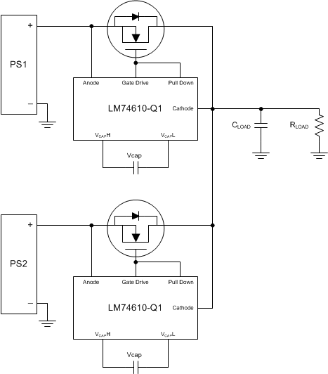 Figure 21. Typical OR-ing Application
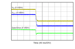
If one of the power supplies fails in LM74610-Q1 OR-ing controller application, the output remains uninterrupted. This behavior is similar to diode OR-ing. Figure 22
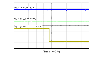 Figure 22. LM74610-Q1 OR-ing waveform
8.2.6 Design Requirements
NOTE
Startup voltage is the voltage drop is needed for the controller to turn ON. It directly influences the Minimum output current at which the MOSFET turns ON.
Table 2. Recommended MOSFET Examples(1)
| Part No | Voltage (V) Current | Drain Current at 25C | Rdson mΩ @ 4.5V | Vgs Threshold(V) | Diode voltage @ 2A at 125C/175C | Package; Footprint | Qual | |
|---|---|---|---|---|---|---|---|---|
| CSD17313Q2Q1 | 30 | 5 | 26 | 1.8 | 0.65 | SON; 2 x 2 | Auto | |
| SQJ886EP | 40 | 60 | 5.5 | 2.5 | 0.5 | PowerPAK SO-8L; 5 x 6 | Auto | |
| SQ4184EY | 40 | 29 | 5.6 | 2.5 | 0.5 | SO-8; 5 x 6 | Auto | |
| Si4122DY | 40 | 23.5 | 6 | 2.5 | 0.5 | SO-8; 5 x 6 | Auto | |
| RS1G120MN | 40 | 12 | 20.7 | 2.5 | 0.6 | HSOP8; 5 x 6 | Auto | |
| RS1G300GN | 40 | 30 | 2.5 | 2.5 | 0.5 | HSOP8; 5 x 6 | Auto | |
| CSD18501Q5A | 40 | 22 | 3.3 | 2.3 | 0.53 | SON; 5 x 6 | Industrial | |
| SQD40N06-14L | 60 | 40 | 17 | 2.5 | 0.5 | TO-252; 6 x 10 | Auto | |
| SQ4850EY | 60 | 12 | 31 | 2.5 | 0.55 | SO-8; 5 x 6 | Auto | |
| CSD18532Q5B | 60 | 23 | 3.3 | 2.2 | 0.53 | SON;5 x 6 | Industrial | |
| IPG20N04S4L-07A | 40 | 20 | 7.2 | 2.2 | 0.48 | PG-TDSON-8-10; 5 x 6 | Auto | |
| IPB057N06N | 60 | 45 | 5.7 | 3.3 | 0.55 | PG-TO263-3; 10 x 15 | Auto | |
| IPD50N04S4L | 40 | 50 | 7.3 | 2.2 | 0.50 | PG-TO252-3-313; 6 x10 | Auto | |
| BUK9Y3R5-40E | 40 | 100 | 3.8 | 2.1 | 0.48 | LFPAK56; Power-SO8 (SOT669); 5 x 6 | Auto | |
| IRF7478PbF-1 | 60 | 7 | 30 | 3 | 0.55 | SO-8; 5 x 6 | Industrial | |
| SQJ422EP | 40 | 75 | 4.3 | 2.5 | 0.50 | PowerPAK SO-8L; 5 x 6 | Auto | |
| IRL1004 | 40 | 130 | 6.5 | 1 | 0.60 | TO-220AB | Auto | |
| AUIRL7736 | 40 | 112 | 2.2 | 3 | 0.65 | DirectFET®; 5 x 6 | Auto | |
Table 3. Recommended TVS Combination to meet ISO7637 Specifications (Note 4)
| TVS + | TVS- |
|---|---|
| SMA6T33AY | SMBJ14A/ SMA6T15AY |
| SMA6T30AY | SMBJ14A/ SMA6T15AY |
| SMA6T28AY | SMBJ14A/ SMA6T15AY |
