SNOSCZ1B July 2015 – June 2016 LM74610-Q1
PRODUCTION DATA.
- 1 Features
- 2 Applications
- 3 Description
- 4 Revision History
- 5 Pin Configuration and Functions
- 6 Specifications
- 7 Detailed Description
- 8 Application and Implementation
- 9 Power Supply Recommendations
- 10Layout
- 11Device and Documentation Support
- 12Mechanical, Packaging, and Orderable Information
パッケージ・オプション
メカニカル・データ(パッケージ|ピン)
- DGK|8
サーマルパッド・メカニカル・データ
- DGK|8
発注情報
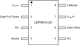
5 Pin Configuration and Functions
DGK Package
8-Pin VSSOP
Top View

Pin Functions
| PIN | DESCRIPTION | |
|---|---|---|
| NO. | NAME | |
| 1 | VcapL | Charge Pump Output, connect to an external charge pump capacitor |
| 2 | Gate Pull Down | Connect to the gate of the external MOSFET for fast turn OFF in the case of reverse polarity |
| 3 | NC | No connect. Leave floating or connect to Anode pin |
| 4 | Anode | Anode of the diode, connect to source of the external MOSFET |
| 5 | NC | No connect. Leave floating or connect to gate drive pin |
| 6 | Gate Drive | Gate Drive output, Connect to the Gate of the external MOSFET |
| 7 | VcapH | Charge Pump Output, connect to an external charge pump capacitor |
| 8 | Cathode | Cathode of the diode, connect to Drain of the external MOSFET |