SNOSCZ1B July 2015 – June 2016 LM74610-Q1
PRODUCTION DATA.
- 1 Features
- 2 Applications
- 3 Description
- 4 Revision History
- 5 Pin Configuration and Functions
- 6 Specifications
- 7 Detailed Description
- 8 Application and Implementation
- 9 Power Supply Recommendations
- 10Layout
- 11Device and Documentation Support
- 12Mechanical, Packaging, and Orderable Information
10 Layout
10.1 Layout Guidelines
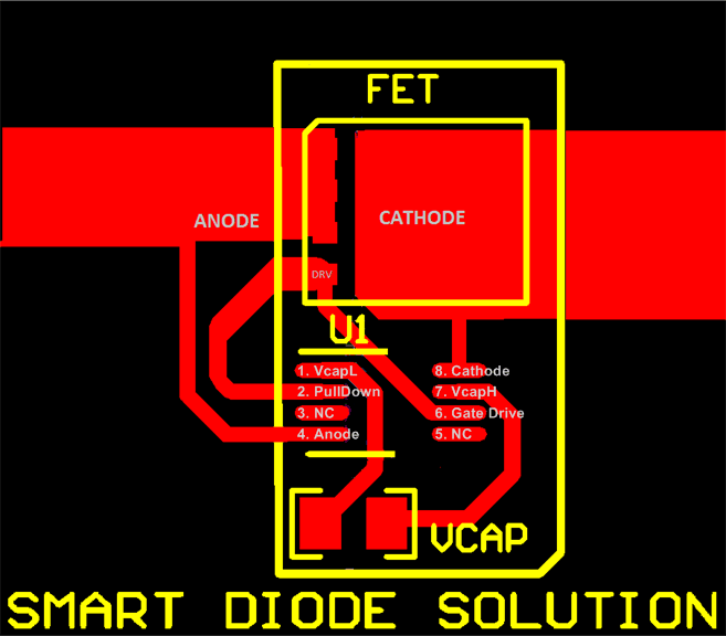
- The VIN terminal is recommended to have a low-ESR ceramic bypass-capacitor. The typical recommended bypass capacitance is a 10-μF ceramic capacitor with a X5R or X7R dielectric.
- The VIN terminal must be tied to the source of the MOSFET using a thick trace or polygon.
- The Anode pin of the LM74610-Q1 is connected to the Source of the MOSFET for sensing.
- The Cathode pin of the LM74610-Q1 is connected to the drain of the MOSFET for sensing.
- The high current path of for this solution is through the MOSFET, therefor it is important to use thick traces for source and drain of the MOSFET.
- The charge pump capacitor Vcap must be kept away from the MOSFET to lower the thermal effects on the capacitance value.
- The Gate Drive and Gate pull down pins of the LM74610-Q1 must be connected to the MOSFET gate without using vias. Avoid excessively thin traces to the Gate Drive.
- Obtaining acceptable performance with alternate layout schemes is possible, however this layout has been shown to produce good results and is intended as a guideline.
- Keep the Drive pin close to the MOSFET to avoid further reduce MOSFET turn-on delay.
10.2 Layout Example
 Figure 23. Layout Example