JAJSBA0Q January 2000 – December 2017 LP2950-N , LP2951-N
PRODUCTION DATA.
- 1 特長
- 2 アプリケーション
- 3 概要
- 4 改訂履歴
- 5 Voltage Options
- 6 Pin Configuration and Functions
- 7 Specifications
-
8 Detailed Description
- 8.1 Overview
- 8.2 Functional Block Diagrams
- 8.3 Feature Description
- 8.4 Device Functional Modes
-
9 Application and Implementation
- 9.1 Application Information
- 9.2
Typical Applications
- 9.2.1 1-A Regulator with 1.2-V Dropout
- 9.2.2 300-mA Regulator with 0.75-V Dropout
- 9.2.3 Wide Input Voltage Range Current Limiter
- 9.2.4 Low Drift Current Source
- 9.2.5 5-V Current Limiter
- 9.2.6 Regulator with Early Warning and Auxiliary Output
- 9.2.7 Latch Off When Error Flag Occurs
- 9.2.8 2-A Low Dropout Regulator
- 9.2.9 5-V Regulator with 2.5-V Sleep Function
- 9.2.10 Open Circuit Detector for 4 → 20-mA Current Loop
- 9.2.11 Regulator with State-of-Charge Indicator
- 9.2.12 Low Battery Disconnect
- 9.2.13 System Overtemperature Protection Circuit
- 10Power Supply Recommendations
- 11Layout
- 12デバイスおよびドキュメントのサポート
- 13メカニカル、パッケージ、および注文情報
パッケージ・オプション
メカニカル・データ(パッケージ|ピン)
サーマルパッド・メカニカル・データ
発注情報
7.7 Typical Characteristics
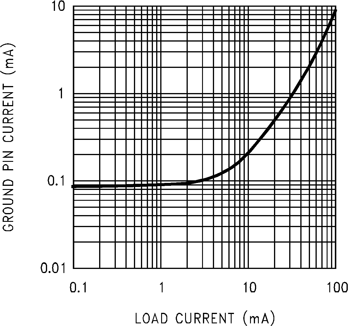 Figure 1. Quiescent Current
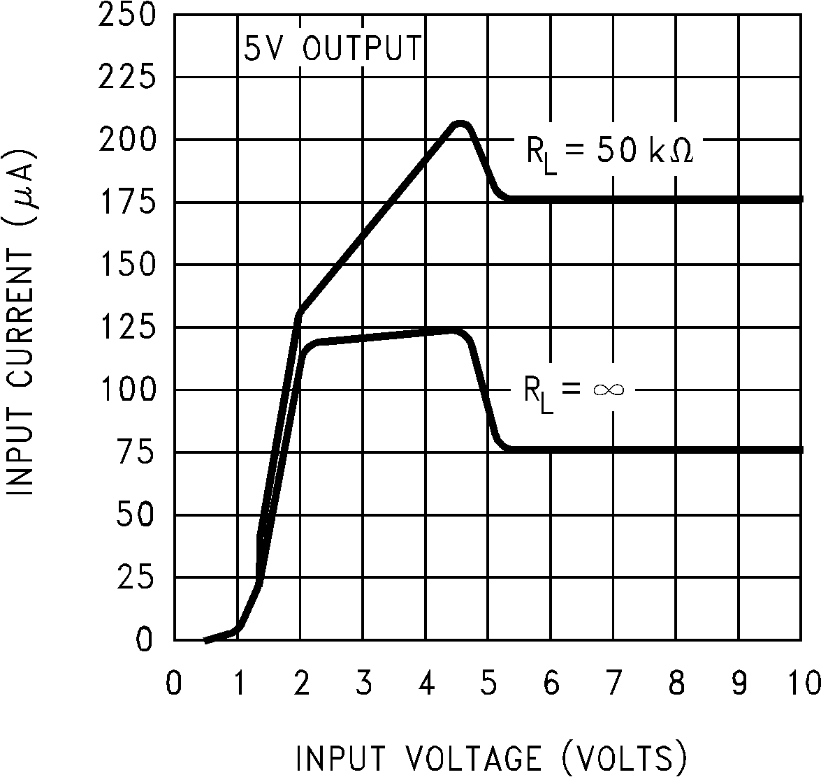 Figure 3. Input Current
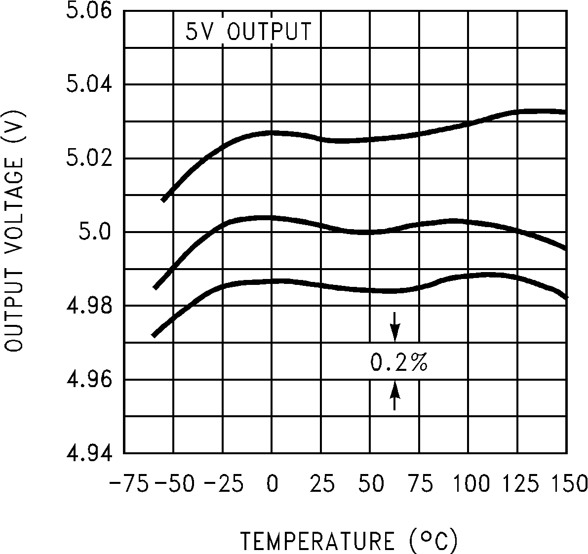 Figure 5. Output Voltage vs. Temperature of 3 Representative Units
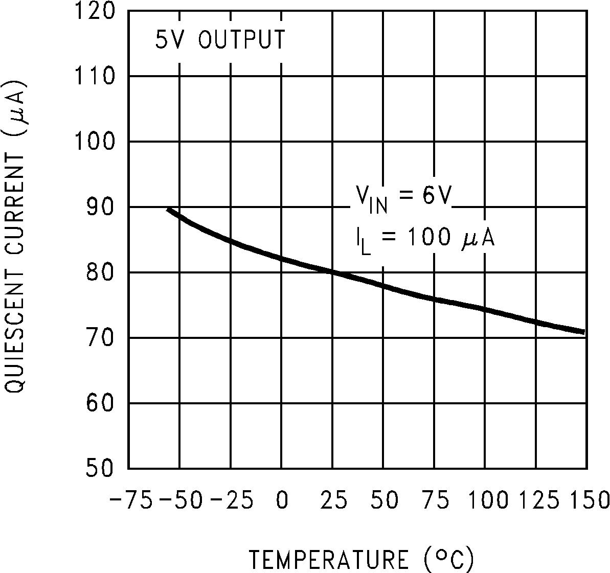 Figure 7. Quiescent Current
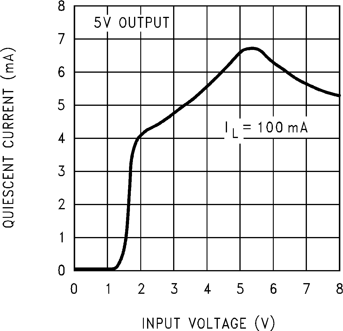 Figure 9. Quiescent Current
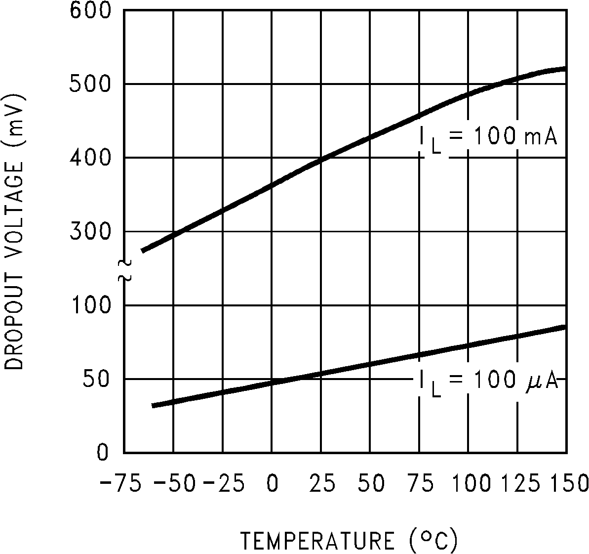 Figure 11. Dropout Voltage
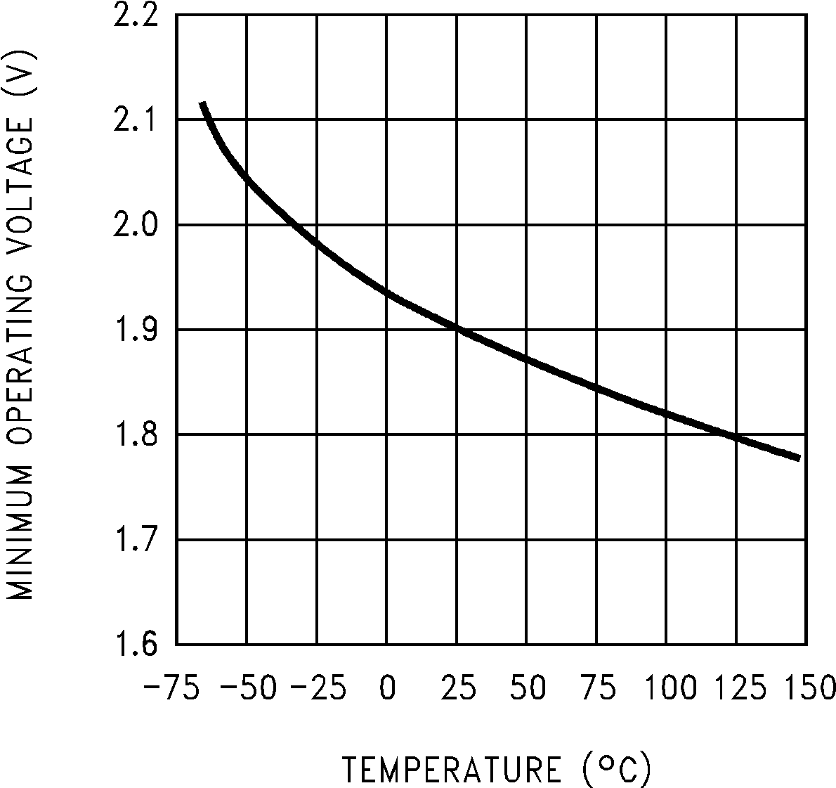 Figure 13. LP2951-N Minimum Operating Voltage
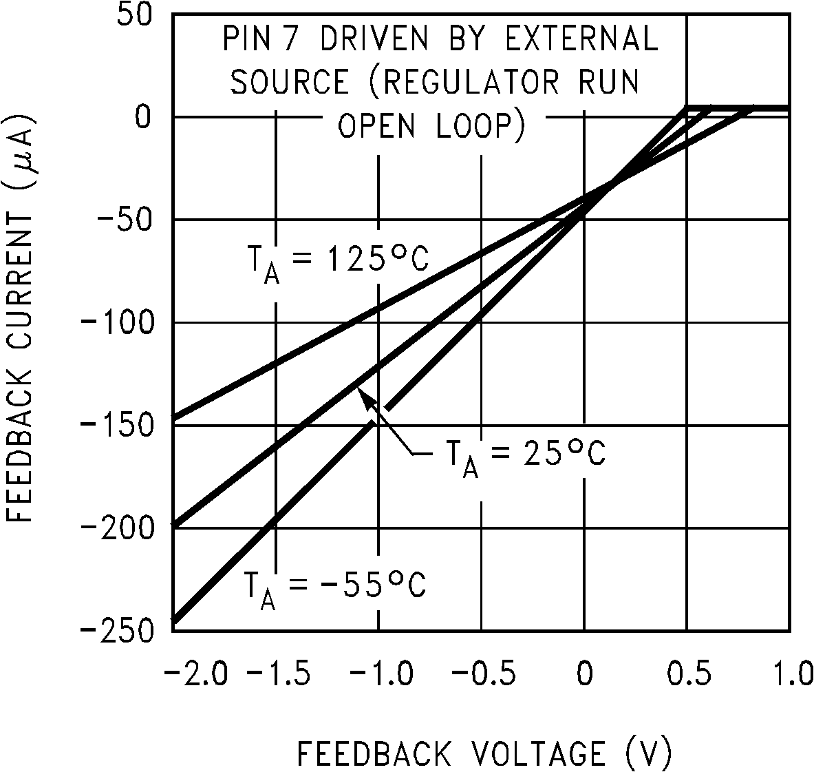 Figure 15. LP2951-N Feedback Pin Current
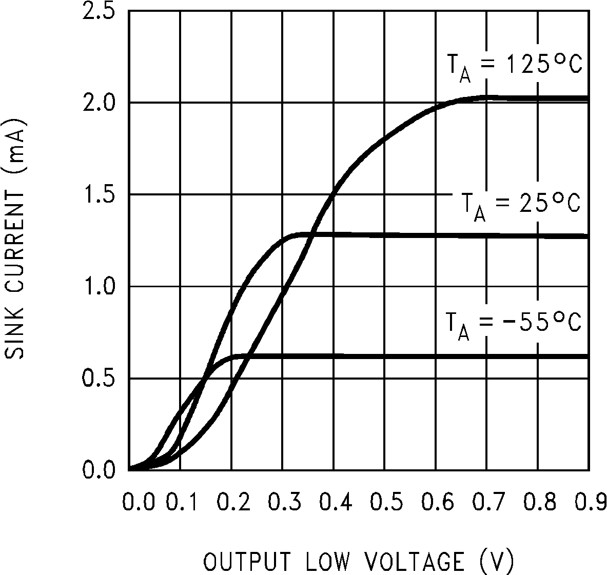 Figure 17. LP2951-N Comparator Sink Current
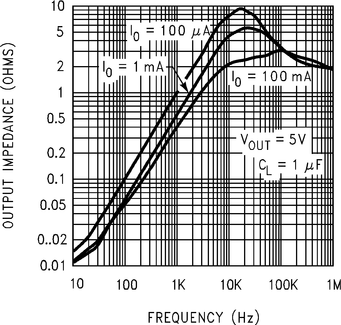 Figure 19. Output Impedance
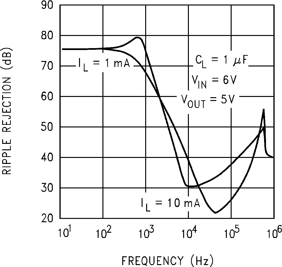 Figure 21. Ripple Rejection
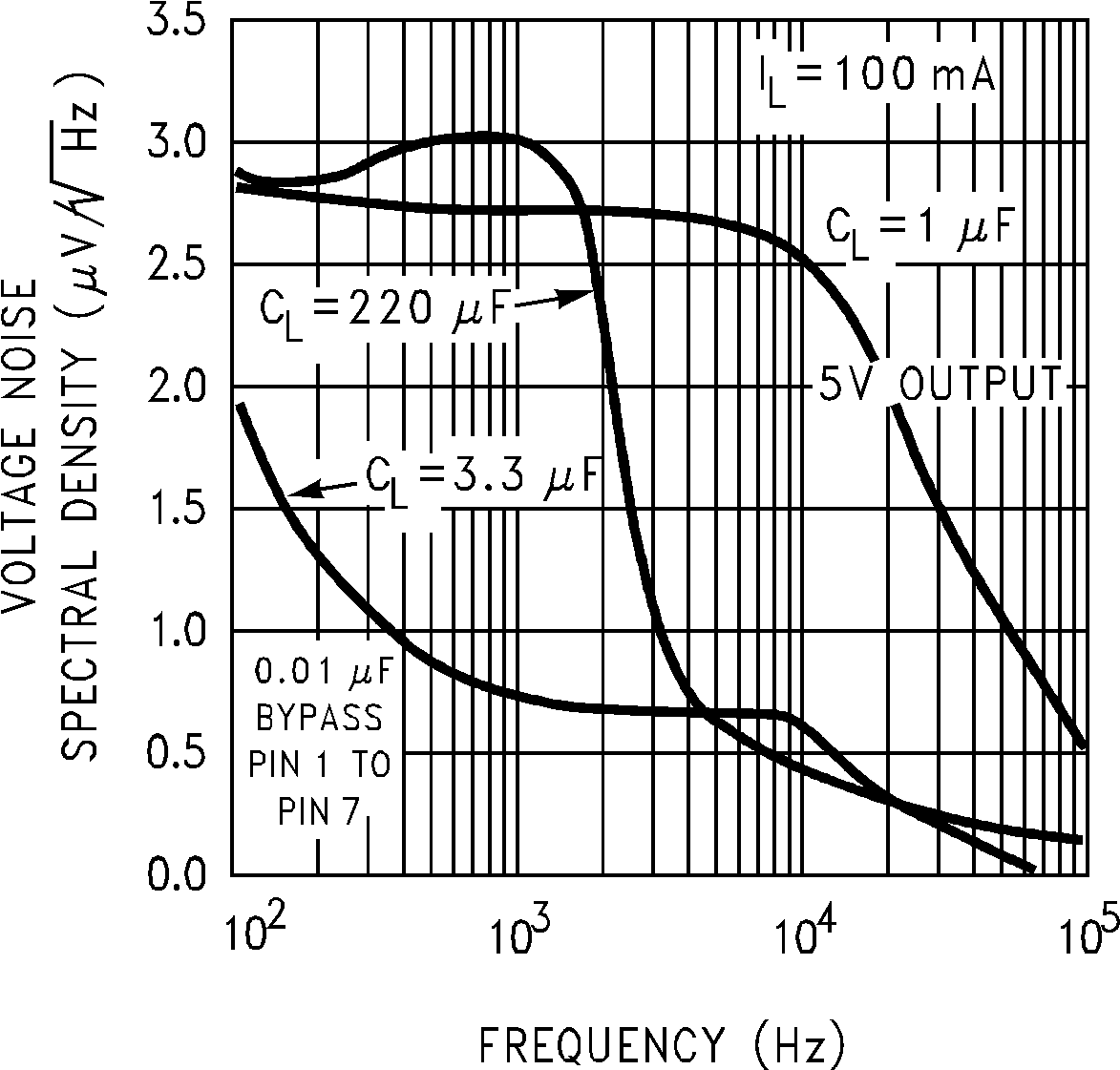 Figure 23. LP2951-N Output Noise
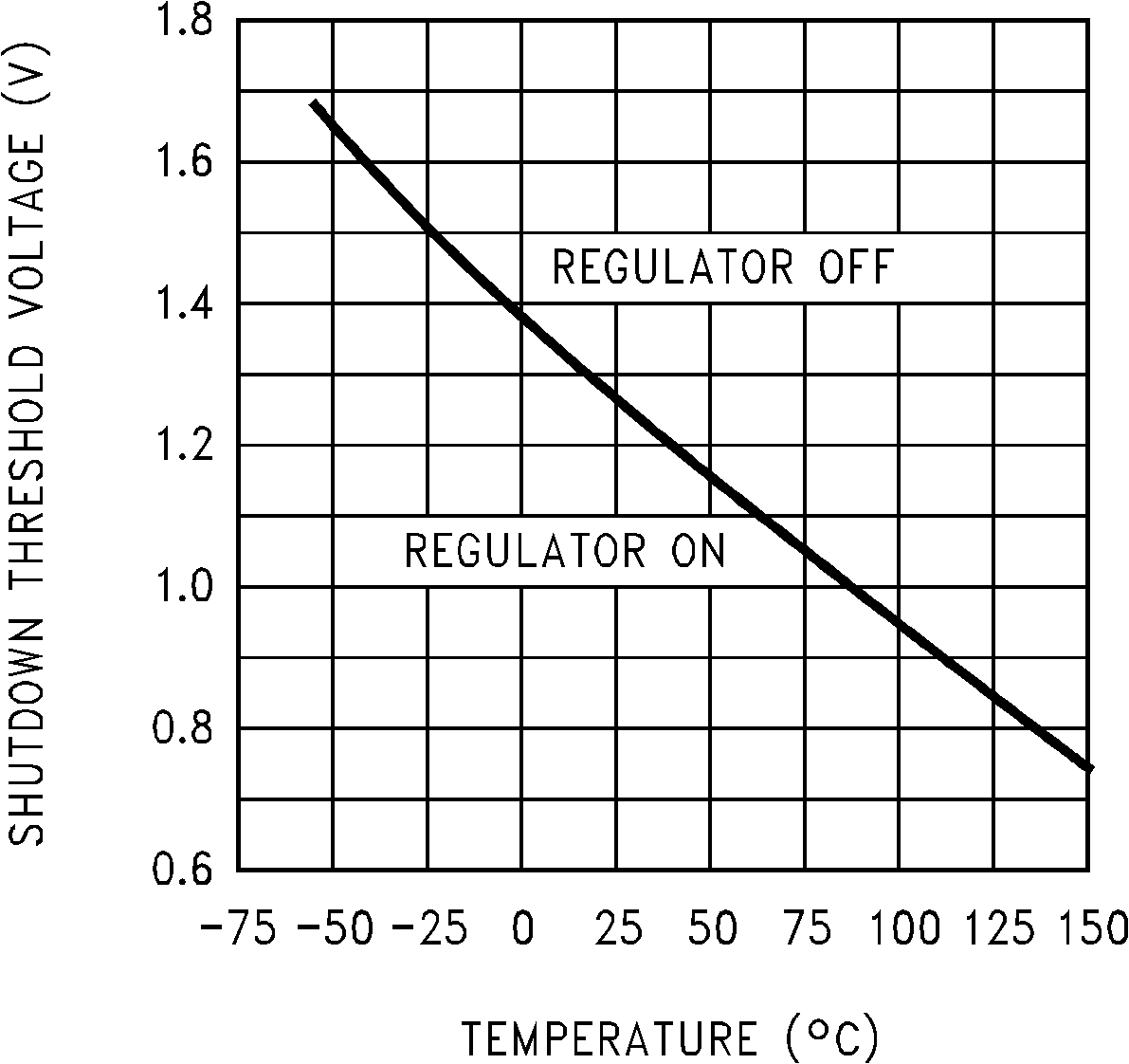 Figure 25. Shutdown Threshold Voltage
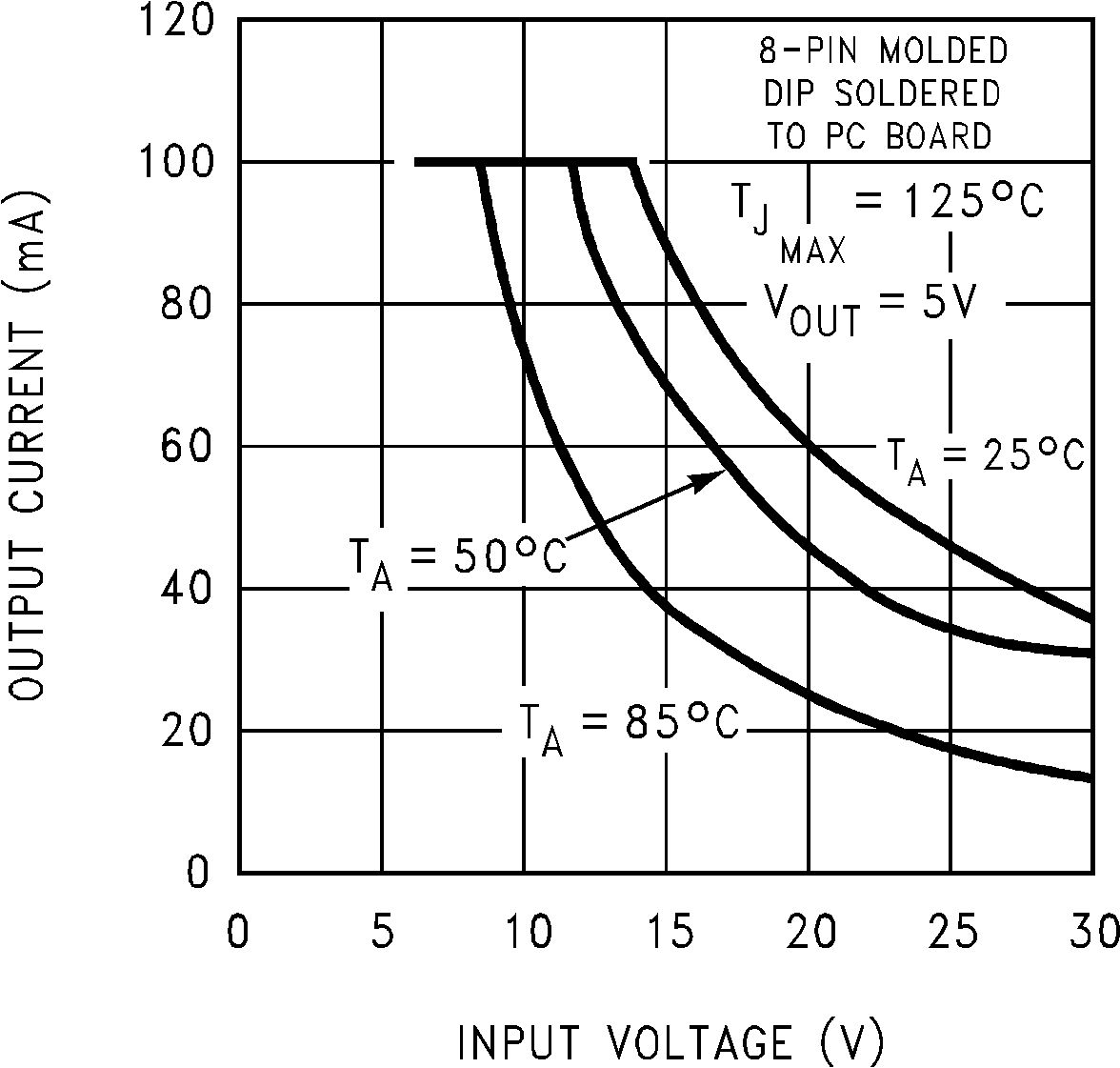 Figure 27. LP2951-N Maximum Rated Output Current
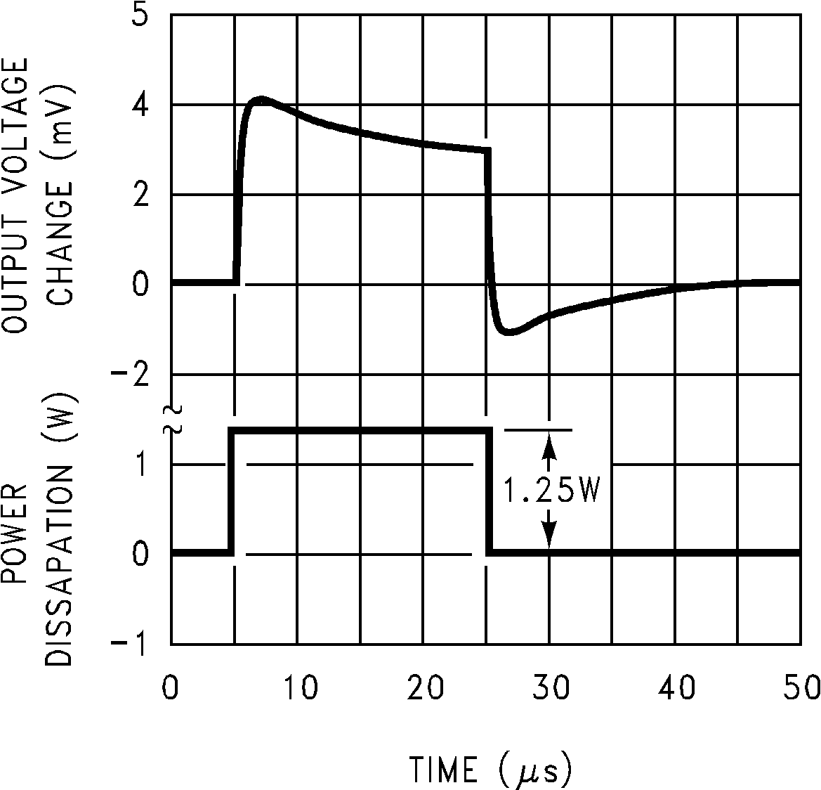 Figure 29. Thermal Response
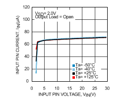 Figure 31. LP2951-N Input Pin Current vs Input Voltage
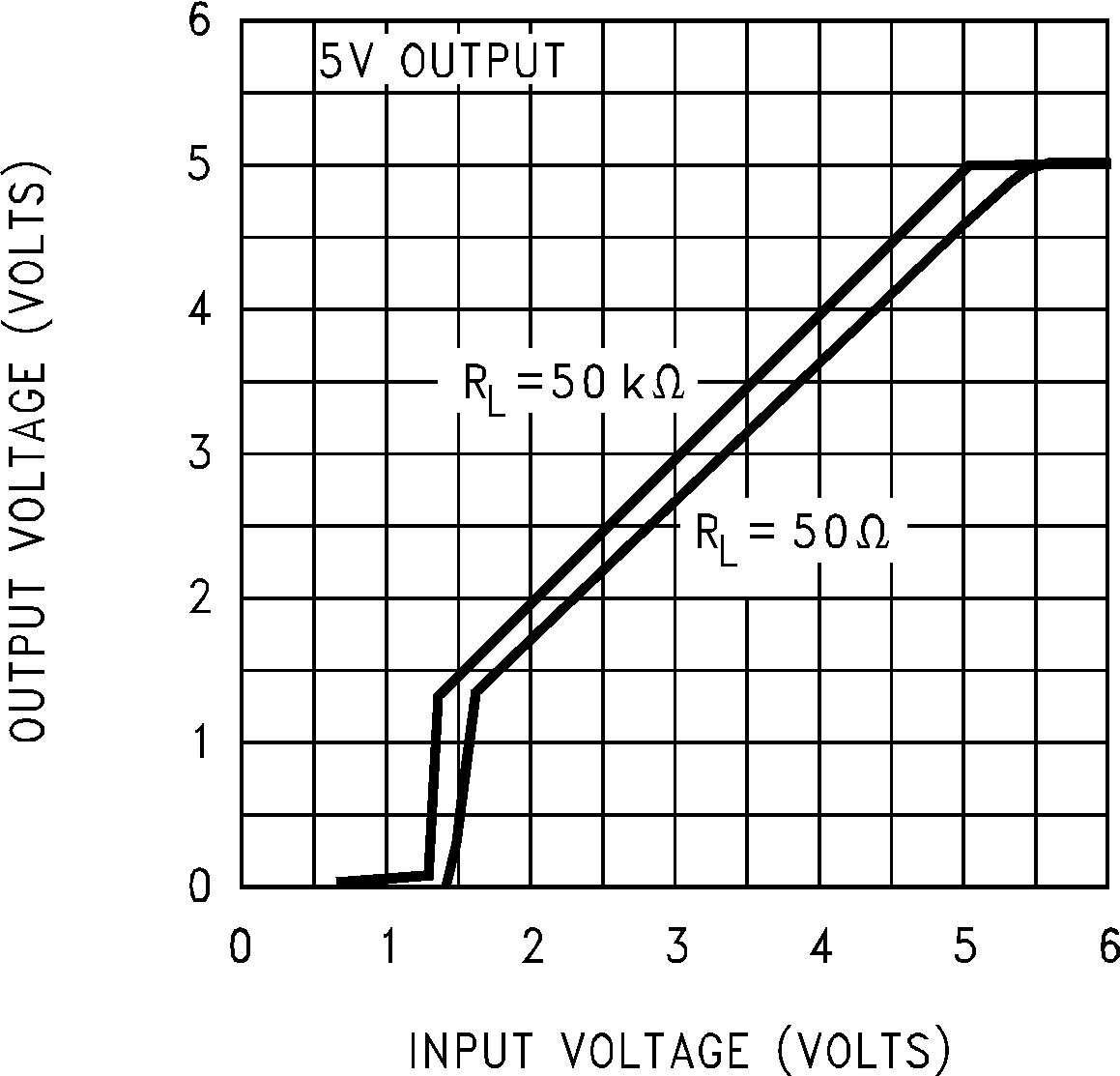 Figure 2. Dropout Characteristics
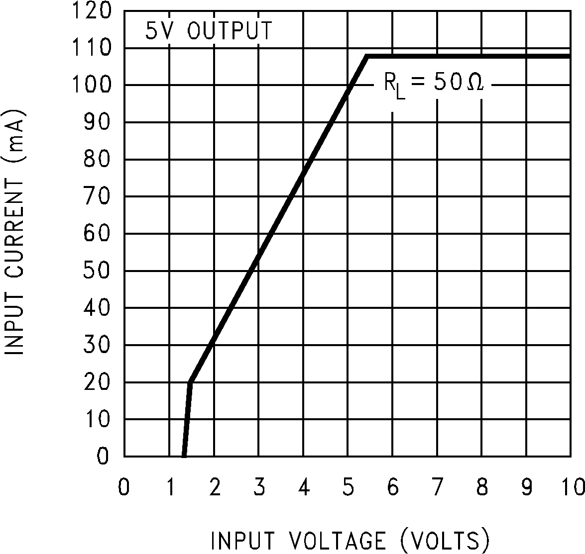 Figure 4. Input Current
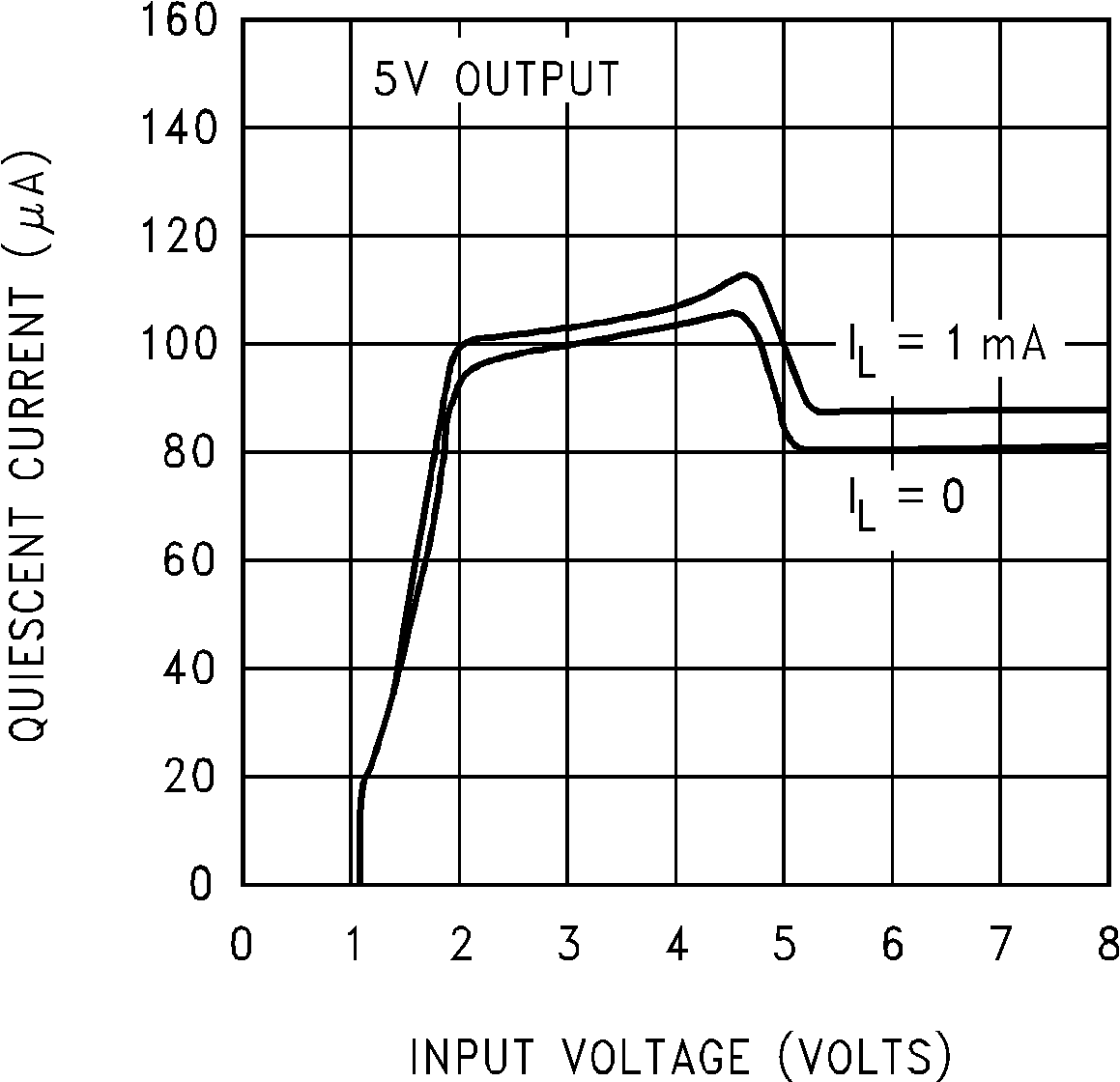 Figure 6. Quiescent Current
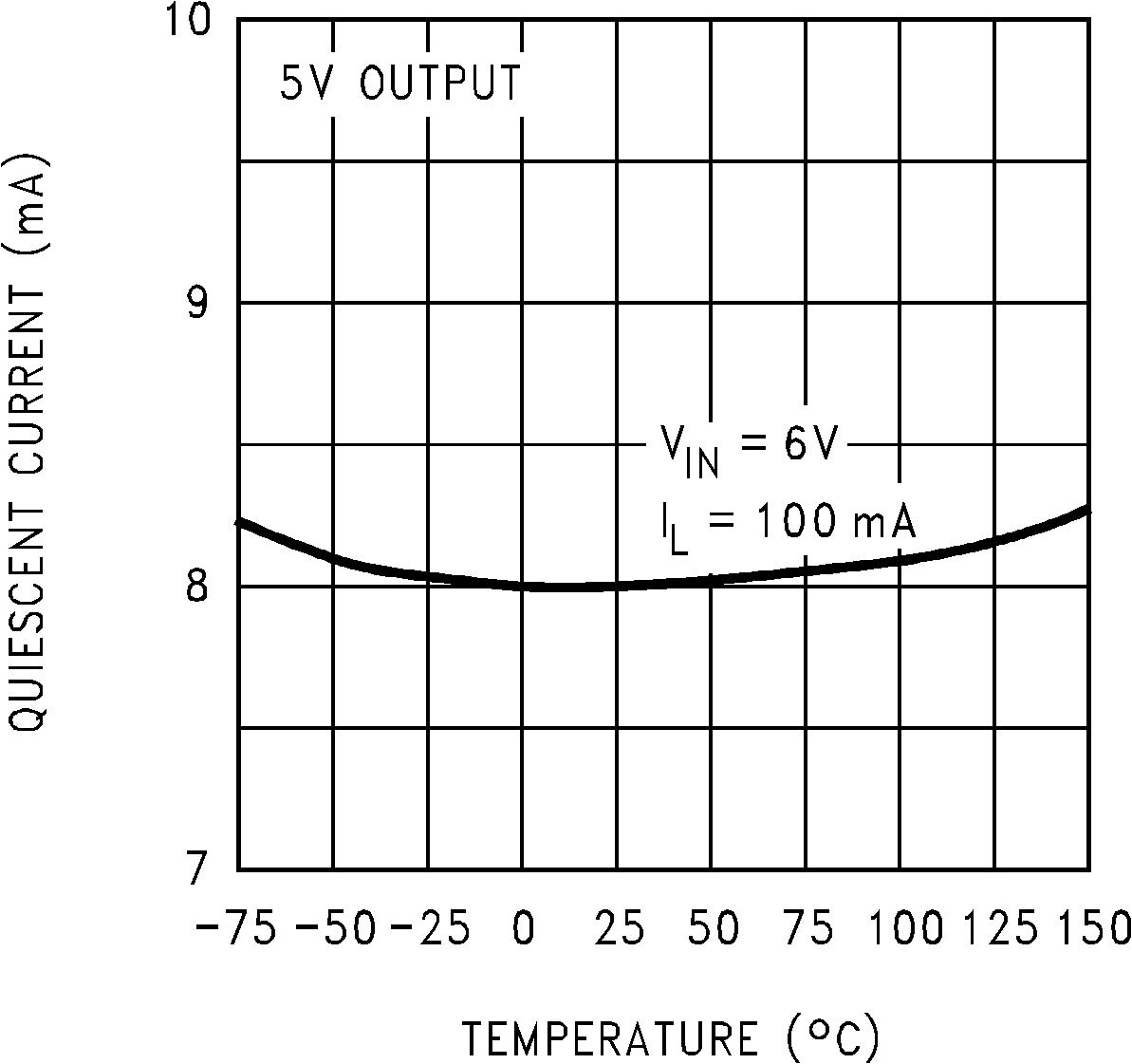 Figure 8. Quiescent Current
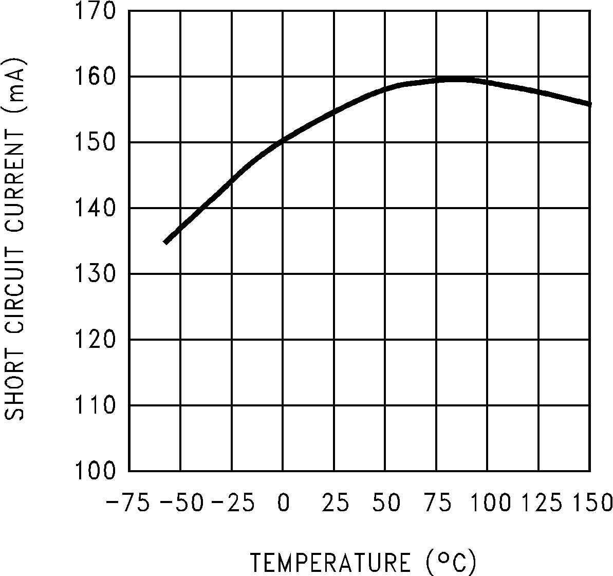 Figure 10. Short Circuit Current
 Figure 12. Dropout Voltage
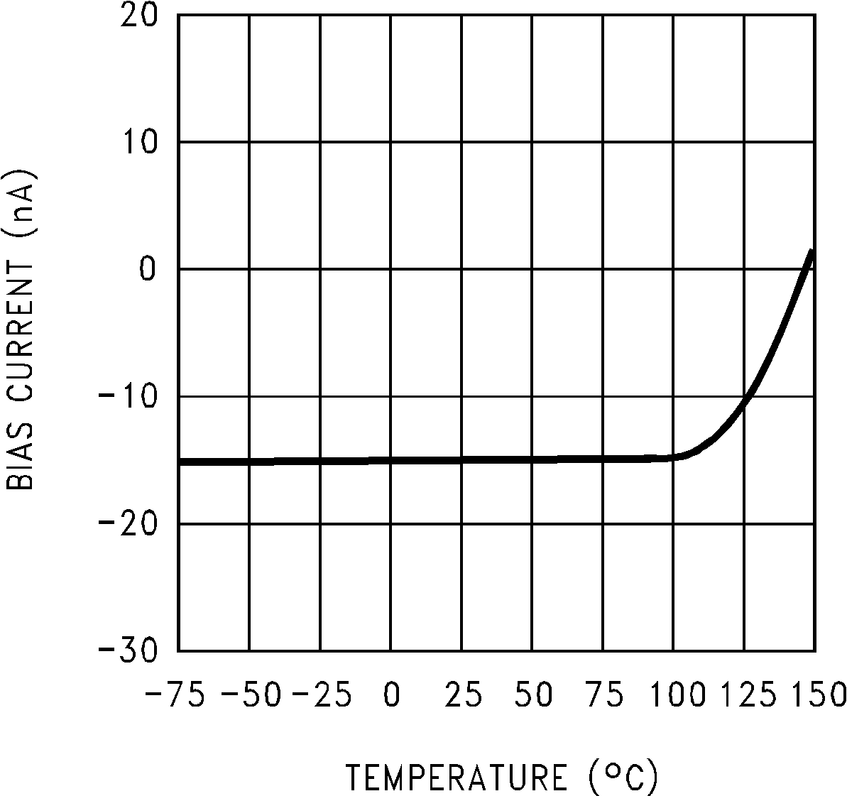 Figure 14. LP2951-N Feedback Bias Current
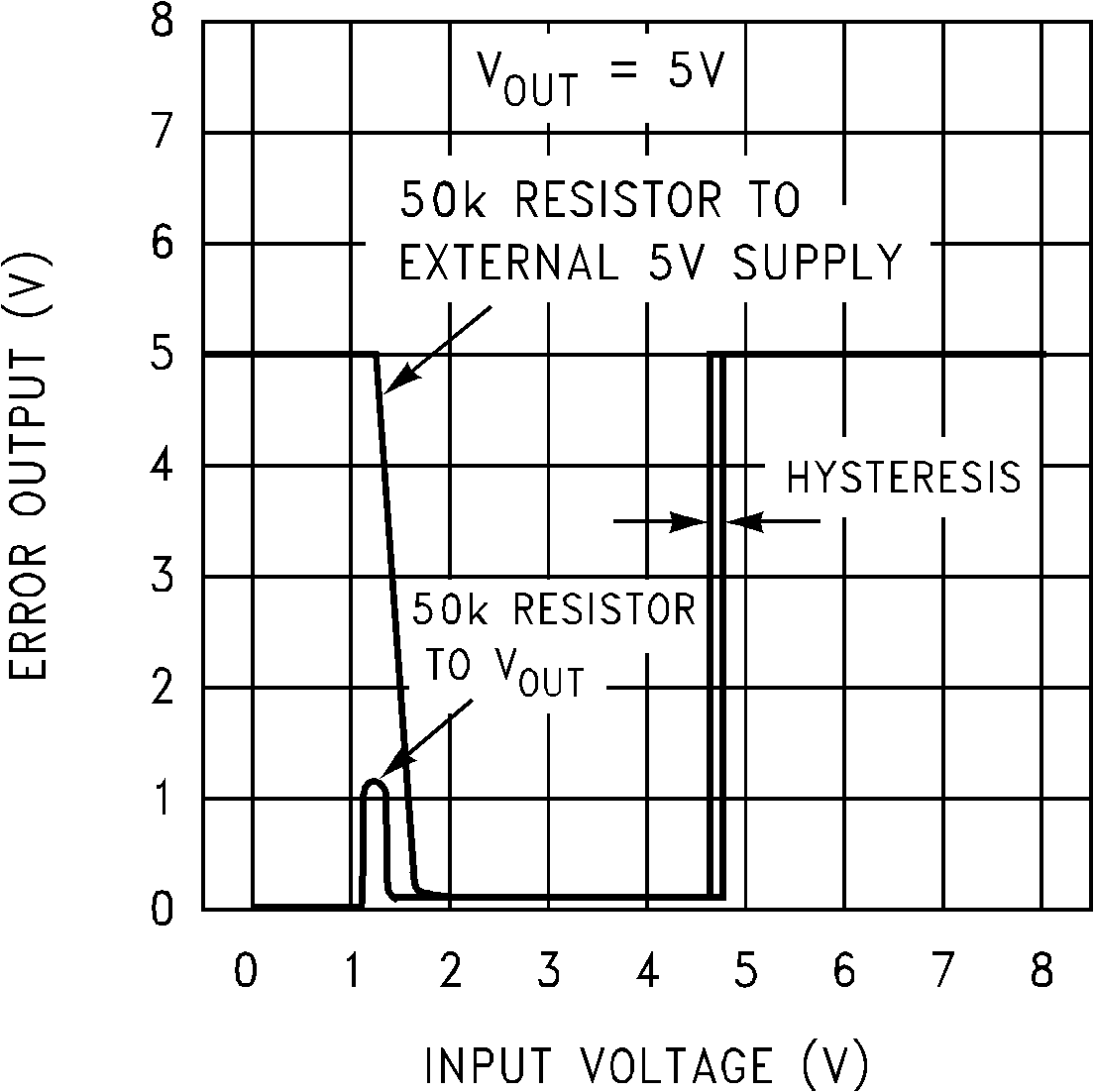 Figure 16. LP2951-N Error Comparator Output
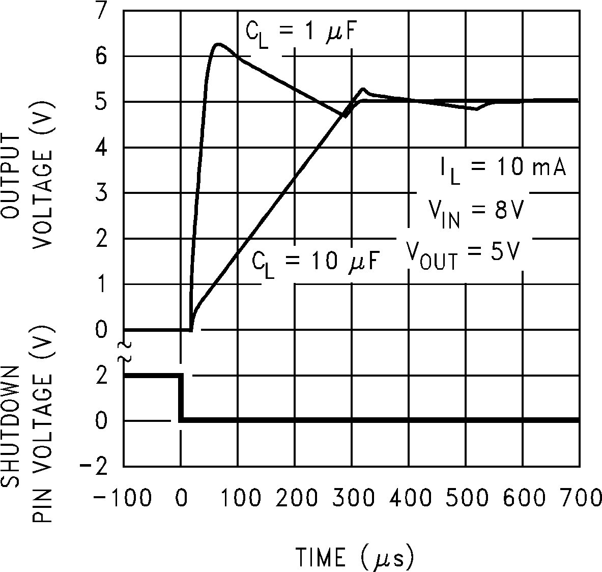 Figure 18. LP2951-N Enable Transient
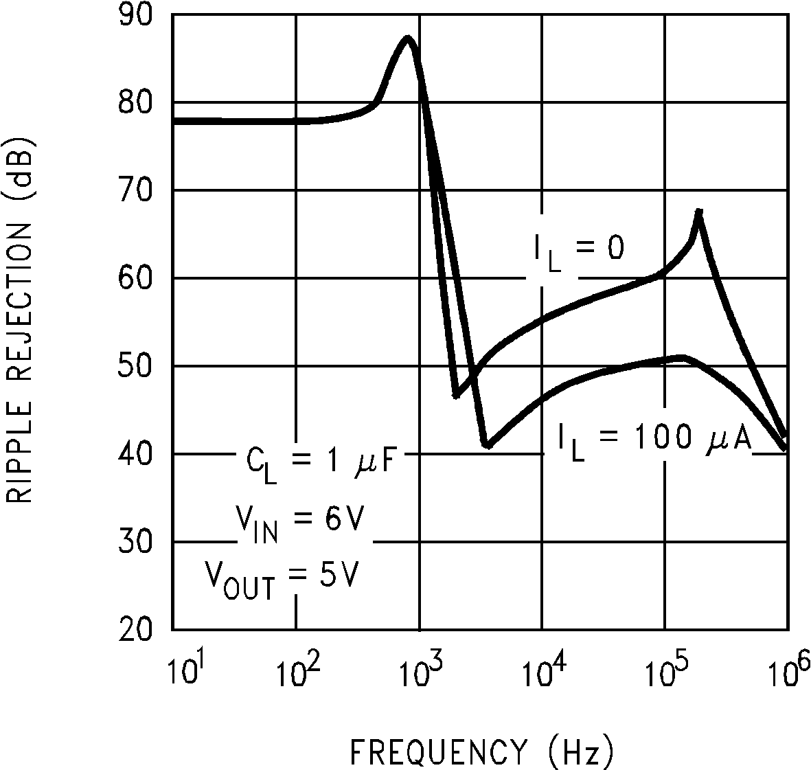 Figure 20. Ripple Rejection
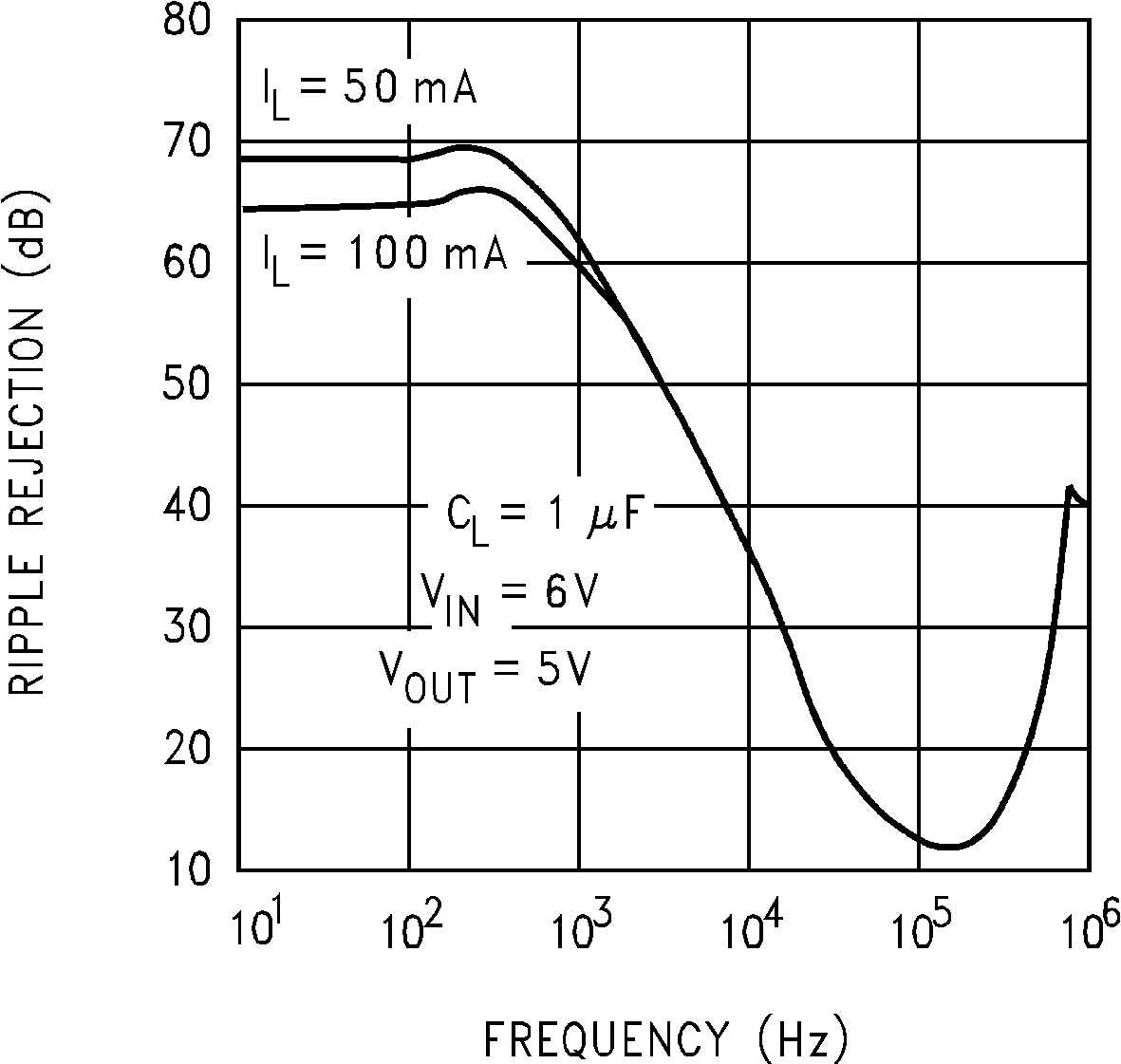 Figure 22. Ripple Rejection
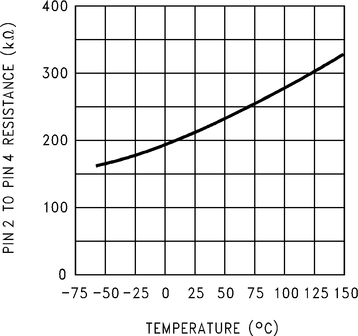 Figure 24. LP2951-N Divider Resistance
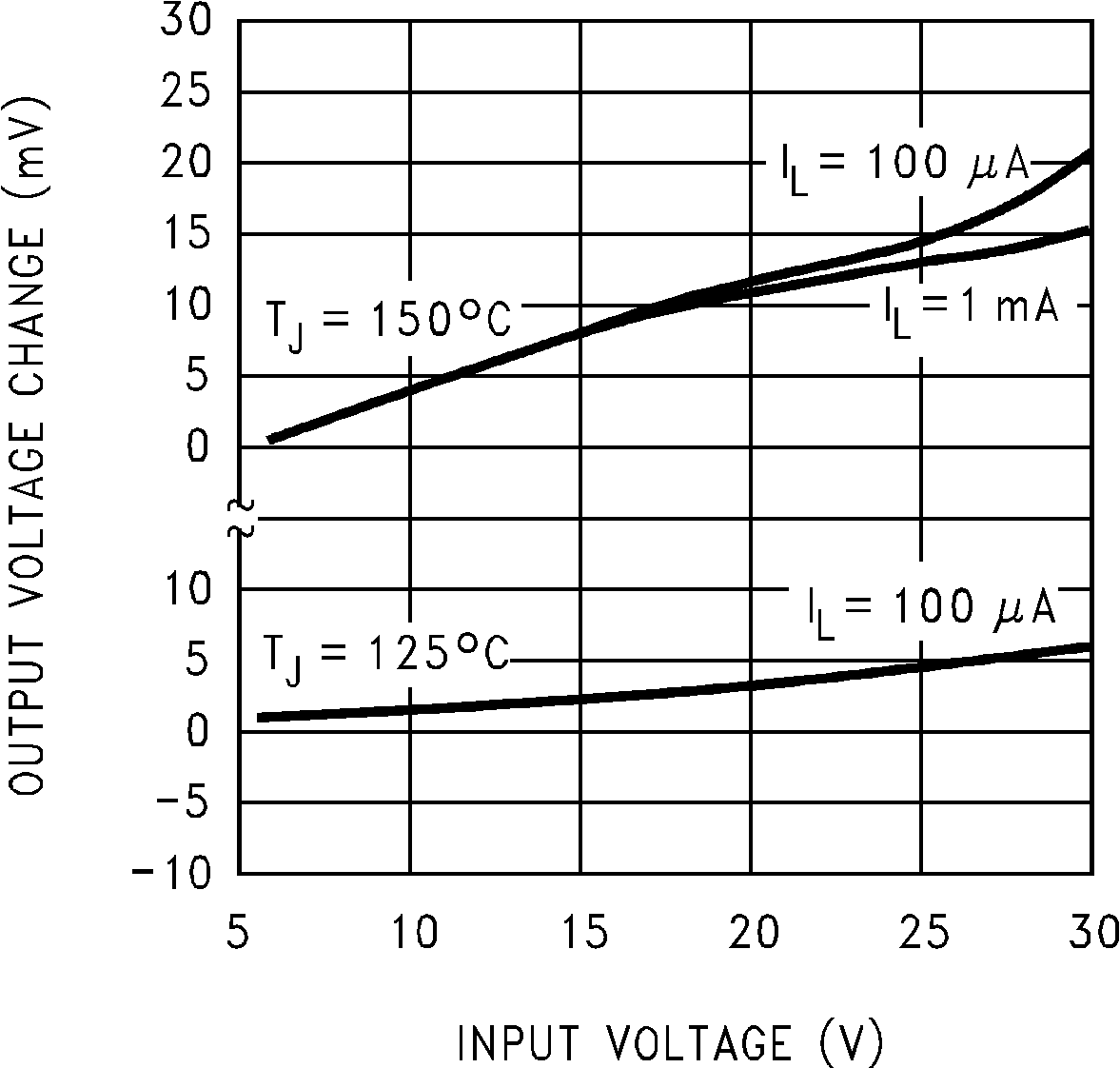 Figure 26. Line Regulation
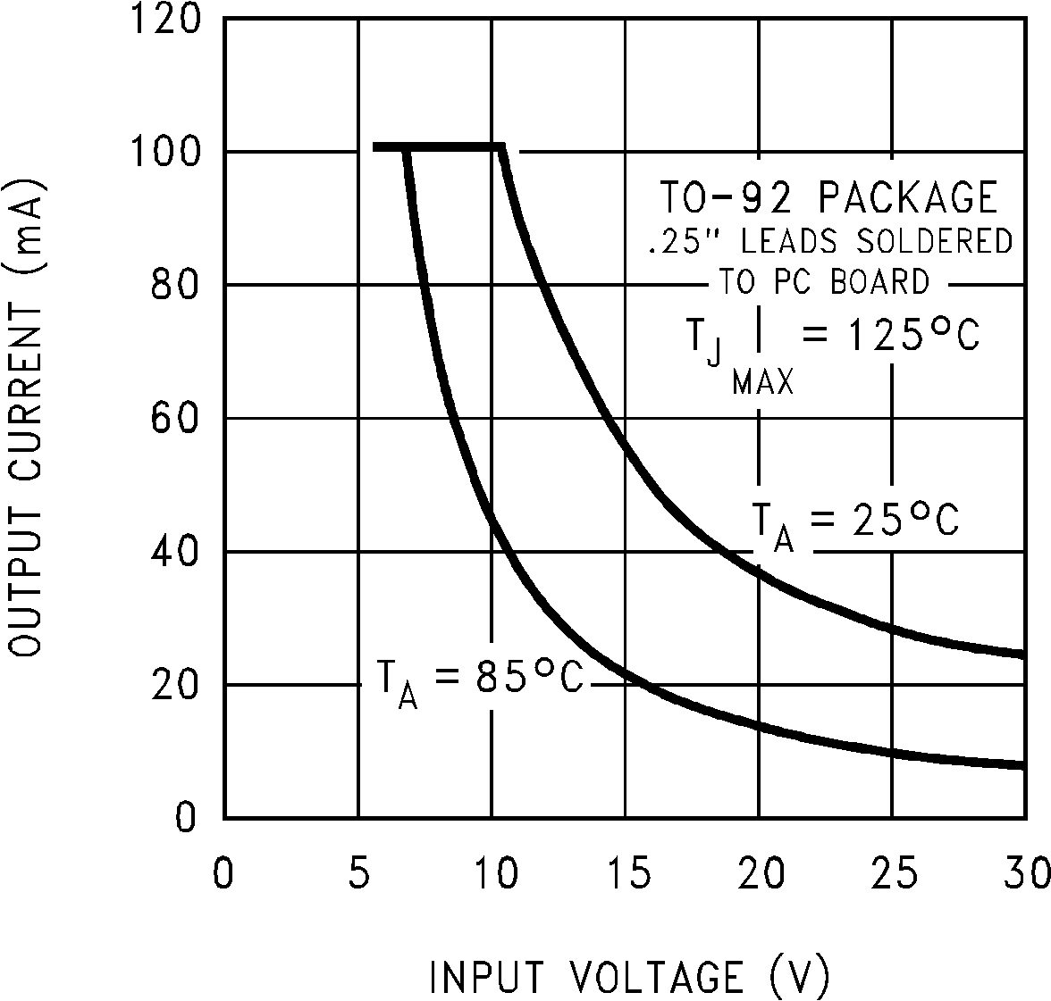 Figure 28. LP2950-N Maximum Rated Output Current
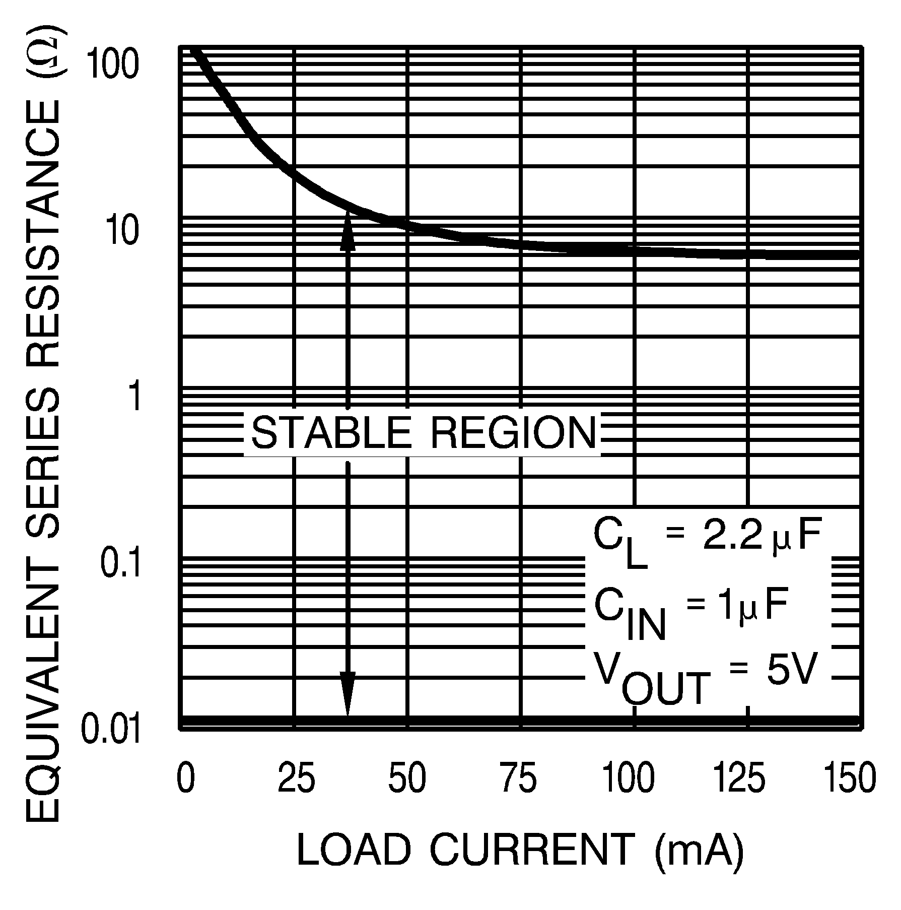 Figure 30. Output Capacitor ESR Range
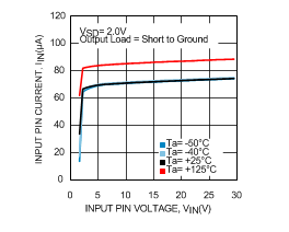 Figure 32. LP2951-N Input Pin Current vs Input Voltage