JAJSBA0Q January 2000 – December 2017 LP2950-N , LP2951-N
PRODUCTION DATA.
- 1 特長
- 2 アプリケーション
- 3 概要
- 4 改訂履歴
- 5 Voltage Options
- 6 Pin Configuration and Functions
- 7 Specifications
-
8 Detailed Description
- 8.1 Overview
- 8.2 Functional Block Diagrams
- 8.3 Feature Description
- 8.4 Device Functional Modes
-
9 Application and Implementation
- 9.1 Application Information
- 9.2
Typical Applications
- 9.2.1 1-A Regulator with 1.2-V Dropout
- 9.2.2 300-mA Regulator with 0.75-V Dropout
- 9.2.3 Wide Input Voltage Range Current Limiter
- 9.2.4 Low Drift Current Source
- 9.2.5 5-V Current Limiter
- 9.2.6 Regulator with Early Warning and Auxiliary Output
- 9.2.7 Latch Off When Error Flag Occurs
- 9.2.8 2-A Low Dropout Regulator
- 9.2.9 5-V Regulator with 2.5-V Sleep Function
- 9.2.10 Open Circuit Detector for 4 → 20-mA Current Loop
- 9.2.11 Regulator with State-of-Charge Indicator
- 9.2.12 Low Battery Disconnect
- 9.2.13 System Overtemperature Protection Circuit
- 10Power Supply Recommendations
- 11Layout
- 12デバイスおよびドキュメントのサポート
- 13メカニカル、パッケージ、および注文情報
パッケージ・オプション
メカニカル・データ(パッケージ|ピン)
サーマルパッド・メカニカル・データ
発注情報
9.2.1.2.1 Output Capacitor Requirements
A 1-µF (or greater) capacitor is required between the output and ground for stability at output voltages of 5 V or higher. At lower output voltages, more capacitance is required (2.2 µF or more is recommended for 3-V and
3.3-V versions). Without this capacitor the device oscillates. Most types of tantalum or aluminum electrolytic work fine here; even film types work but are not recommended for reasons of cost. Many aluminum electrolytics have electrolytes that freeze at about −30°C, so solid tantalums are recommended for operation below −25°C. The important parameters of the capacitor are an ESR of about 5 Ω or less and a resonant frequency above 500 kHz. The value of this capacitor may be increased without limit.
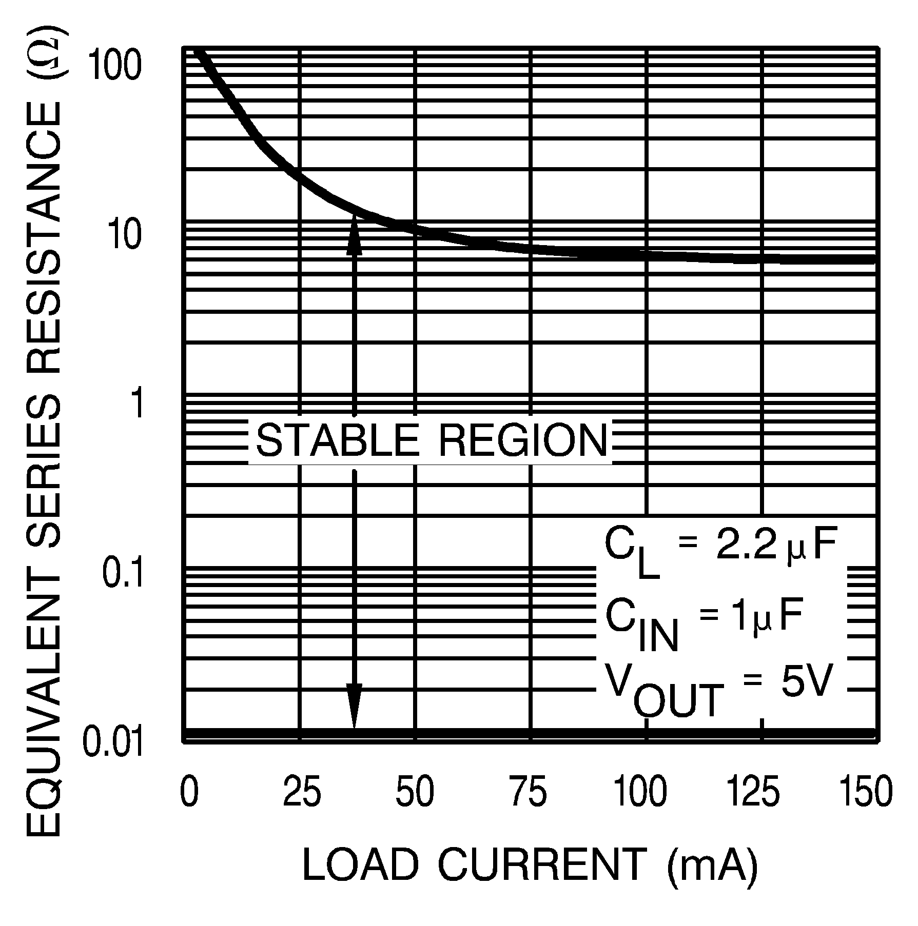
 Figure 37. Output Capacitor ESR Range
The reason for the lower ESR limit is that the loop compensation of the feedback loop relies on the capacitance value and the ESR value of the output capacitor to provide the zero that gives added phase lead (See Figure 37).
Using the 2.2 µF value from the Output Capacitor ESR Range curve (Figure 37), a useful range for fZ can be estimated:
For ceramic capacitors, the low ESR produces a zero at a frequency that is too high to be useful, so meaningful phase lead does not occur. A ceramic output capacitor can be used if a series resistance is added (recommended value of resistance about 0.1 Ω to 2 Ω) to simulate the needed ESR. Only X5R, X7R, or better, MLCC types should be used, and should have a DC voltage rating at least twice the VOUT(NOM) value.
At lower values of output current, less output capacitance is required for stability. The capacitor can be reduced to 0.33 µF for currents below 10 mA or 0.1 µF for currents below 1 mA. Using the adjustable versions at voltages below 5 V runs the error amplifier at lower gains so that more output capacitance is needed. For the worst-case situation of a 100-mA load at 1.23 V output (output shorted to Feedback) a 3.3-µF (or greater) capacitor should be used.
Unlike many other regulators, the LP2950-N remains stable and in regulation with no load in addition to the internal voltage divider. This is especially important in CMOS RAM keep-alive applications. When setting the output voltage of the LP2951-N versions with external resistors, a minimum load of 1 µA is recommended.
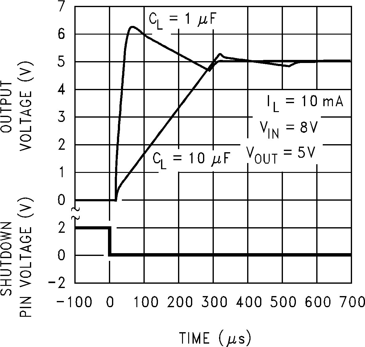
Applications having conditions that may drive the LP2950-N/51 into nonlinear operation require special consideration. Nonlinear operation occurs when the output voltage is held low enough to force the output stage into output current limiting while trying to pull the output voltage up to the regulated value. The internal loop response time controls how long it takes for the device to regain linear operation when the output has returned to the normal operating range. There are three significant nonlinear conditions that need to be considered, all can force the output stage into output current limiting mode, all can cause the output voltage to over-shoot with low value output capacitors when the condition is removed, and the recommended generic solution is to set the output capacitor to a value not less than 10 µF. Although the 10 µF value for COUT may not eliminate the output voltage over-shoot in all cases, it should lower it to acceptable levels (< 10% of VOUT(NOM)) in the majority of cases. In all three of these conditions, applications with lighter load currents are more susceptible to output voltage over-shoot than applications with higher load currents.
- At power-up, with the input voltage rising faster than output stage can charge the output capacitor.
- ΔVIN = VOUT(NOM) + 1 V
- Recovery from an output short circuit to ground condition.
- Toggling the LP2951-N SHUTDOWN pin from high (OFF) to low (ON).
where
 Figure 38. LP2951-N Enable Transient