JAJSBA0Q January 2000 – December 2017 LP2950-N , LP2951-N
PRODUCTION DATA.
- 1 特長
- 2 アプリケーション
- 3 概要
- 4 改訂履歴
- 5 Voltage Options
- 6 Pin Configuration and Functions
- 7 Specifications
-
8 Detailed Description
- 8.1 Overview
- 8.2 Functional Block Diagrams
- 8.3 Feature Description
- 8.4 Device Functional Modes
-
9 Application and Implementation
- 9.1 Application Information
- 9.2
Typical Applications
- 9.2.1 1-A Regulator with 1.2-V Dropout
- 9.2.2 300-mA Regulator with 0.75-V Dropout
- 9.2.3 Wide Input Voltage Range Current Limiter
- 9.2.4 Low Drift Current Source
- 9.2.5 5-V Current Limiter
- 9.2.6 Regulator with Early Warning and Auxiliary Output
- 9.2.7 Latch Off When Error Flag Occurs
- 9.2.8 2-A Low Dropout Regulator
- 9.2.9 5-V Regulator with 2.5-V Sleep Function
- 9.2.10 Open Circuit Detector for 4 → 20-mA Current Loop
- 9.2.11 Regulator with State-of-Charge Indicator
- 9.2.12 Low Battery Disconnect
- 9.2.13 System Overtemperature Protection Circuit
- 10Power Supply Recommendations
- 11Layout
- 12デバイスおよびドキュメントのサポート
- 13メカニカル、パッケージ、および注文情報
パッケージ・オプション
メカニカル・データ(パッケージ|ピン)
サーマルパッド・メカニカル・データ
発注情報
9.2.1.2.3 Error Detection Comparator Output
The comparator produces a logic low output whenever the LP2951-N output falls out of regulation by more than approximately 5%. This figure is the comparator's built-in offset of about 60 mV divided by the 1.235 reference voltage. (Refer to the block diagram in the front of the datasheet.) This trip level remains “5% below normal” regardless of the programmed output voltage of the 2951. For example, the error flag trip level is typically 4.75 V for a 5-V output or 11.4 V for a 12-V output. The out of regulation condition may be due either to low input voltage, current limiting, or thermal limiting.
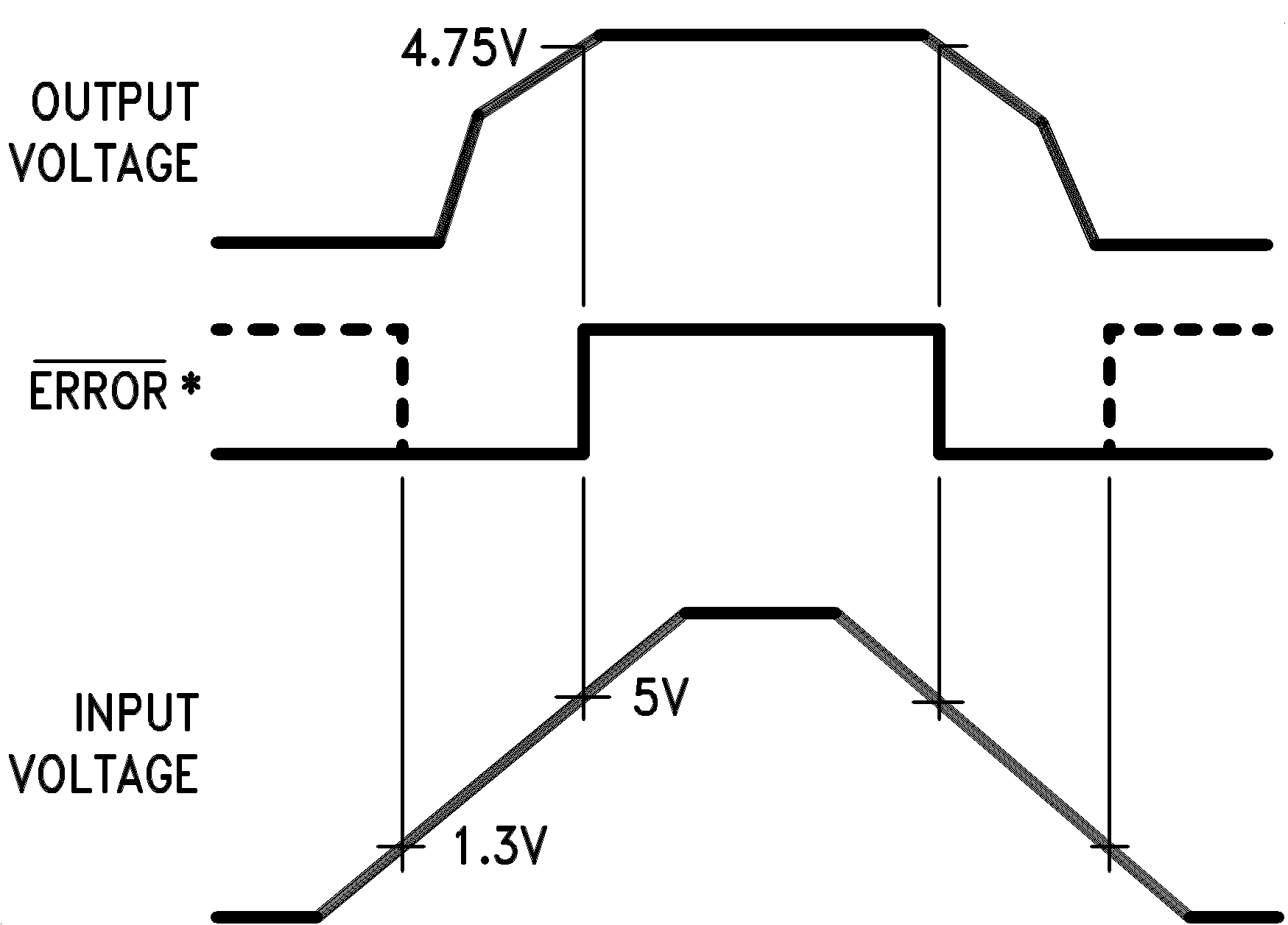
Figure 39 below gives a timing diagram depicting the ERROR signal and the regulated output voltage as the LP2951-N input is ramped up and down. For 5 V versions, the ERROR signal becomes valid (low) at about 1.3-V input. It goes high at about 5-V input (the input voltage at which VOUT = 4.75 V). Because the LP2951-N dropout voltage is load-dependent (see curve in typical performance characteristics), the input voltage trip point (about 5 V) varies with the load current. The output voltage trip point (approx. 4.75 V) does not vary with load.
The error comparator has an open-collector output which requires an external pull up resistor. This resistor may be returned to the output or some other supply voltage depending on system requirements. In determining a value for this resistor, note that while the output is rated to sink 400 µA, this sink current adds to battery drain in a low battery condition. Suggested values range from 100 k to 1 MΩ. The resistor is not required if this output is unused.
