JAJSBA0Q January 2000 – December 2017 LP2950-N , LP2951-N
PRODUCTION DATA.
- 1 特長
- 2 アプリケーション
- 3 概要
- 4 改訂履歴
- 5 Voltage Options
- 6 Pin Configuration and Functions
- 7 Specifications
-
8 Detailed Description
- 8.1 Overview
- 8.2 Functional Block Diagrams
- 8.3 Feature Description
- 8.4 Device Functional Modes
-
9 Application and Implementation
- 9.1 Application Information
- 9.2
Typical Applications
- 9.2.1 1-A Regulator with 1.2-V Dropout
- 9.2.2 300-mA Regulator with 0.75-V Dropout
- 9.2.3 Wide Input Voltage Range Current Limiter
- 9.2.4 Low Drift Current Source
- 9.2.5 5-V Current Limiter
- 9.2.6 Regulator with Early Warning and Auxiliary Output
- 9.2.7 Latch Off When Error Flag Occurs
- 9.2.8 2-A Low Dropout Regulator
- 9.2.9 5-V Regulator with 2.5-V Sleep Function
- 9.2.10 Open Circuit Detector for 4 → 20-mA Current Loop
- 9.2.11 Regulator with State-of-Charge Indicator
- 9.2.12 Low Battery Disconnect
- 9.2.13 System Overtemperature Protection Circuit
- 10Power Supply Recommendations
- 11Layout
- 12デバイスおよびドキュメントのサポート
- 13メカニカル、パッケージ、および注文情報
パッケージ・オプション
メカニカル・データ(パッケージ|ピン)
サーマルパッド・メカニカル・データ
発注情報
9.2.1.2.4 Programming the Output Voltage (LP2951-N)
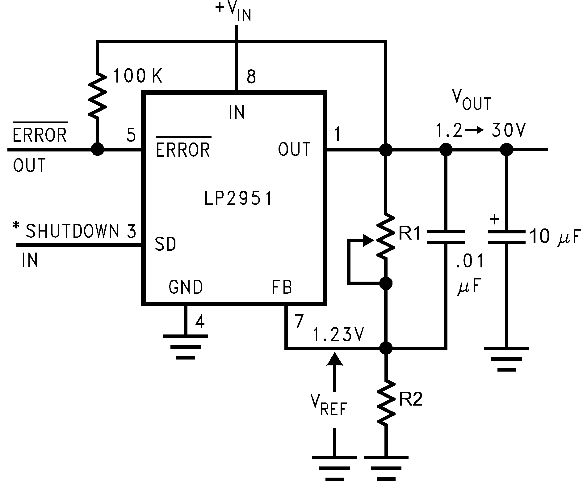
The LP2951-N may be pin-strapped for the nominal fixed output voltage using its internal voltage divider by tying the output and sense pins together, and also tying the FEEDBACK and VTAP pins together. Alternatively, it may be programmed for any output voltage between its 1.235-V reference and its 30-V maximum rating. As seen in Figure 40, an external pair of resistors is required.
The complete equation for the output voltage is

where
- VREF is the nominal 1.235-V reference voltage and IFB is the FEEDBACK pin bias current, nominally –20 nA
The minimum recommended load current of 1 µA forces an upper limit of 1.2 MΩ on the value of R2, if the regulator must work with no load (a condition often found in CMOS in standby). IFB produces a 2% typical error in VOUT which may be eliminated at room temperature by trimming R1. For better accuracy, choosing R2 = 100 kΩ reduces this error to 0.17% while increasing the resistor program current to 12 µA. Because the LP2951-N typically draws 60 µA at no load with pin 2 open-circuited, this is a small price to pay.


*Drive with TTL-high to shut down. Ground or leave open if shutdown feature is not to be used.
Note: Pins 2 and 6 are left open.
Stray capacitance to the LP2951-N FEEDBACK pin can cause instability. This may especially be a problem when using high value external resistors to set the output voltage. Adding a 100-pF capacitor between the OUT pin and the FEEDBACK pin, and increasing the output capacitor to at least 3.3 µF, fixes this problem.