JAJSLG8A October 2019 – February 2021 MSP430F5438A-ET
PRODUCTION DATA
- 1特長
- 2アプリケーション
- 3説明
- 4機能ブロック図
- 5Revision History
- 6Terminal Configuration and Functions
-
7Specifications
- 7.1 Absolute Maximum Ratings
- 7.2 Recommended Operating Conditions
- 7.3 Active Mode Supply Current Into VCC Excluding External Current
- 7.4 Low-Power Mode Supply Currents (Into VCC) Excluding External Current
- 7.5 Thermal Resistance Characteristics
- 7.6 Schmitt-Trigger Inputs – General Purpose I/O
- 7.7 Inputs – Ports P1 and P2
- 7.8 Leakage Current – General Purpose I/O
- 7.9 Outputs – General Purpose I/O (Full Drive Strength)
- 7.10 Outputs – General Purpose I/O (Reduced Drive Strength)
- 7.11 Output Frequency – General Purpose I/O
- 7.12 Typical Characteristics – Outputs, Reduced Drive Strength (PxDS.y = 0)
- 7.13 Typical Characteristics – Outputs, Full Drive Strength (PxDS.y = 1)
- 7.14 Crystal Oscillator, XT1, Low-Frequency Mode
- 7.15 Crystal Oscillator, XT1, High-Frequency Mode
- 7.16 Crystal Oscillator, XT2
- 7.17 Internal Very-Low-Power Low-Frequency Oscillator (VLO)
- 7.18 Internal Reference, Low-Frequency Oscillator (REFO)
- 7.19 DCO Frequency
- 7.20 PMM, Brownout Reset (BOR)
- 7.21 PMM, Core Voltage
- 7.22 PMM, SVS High Side
- 7.23 PMM, SVM High Side
- 7.24 PMM, SVS Low Side
- 7.25 PMM, SVM Low Side
- 7.26 Wakeup From Low-Power Modes and Reset
- 7.27 Timer_A
- 7.28 Timer_B
- 7.29 USCI (UART Mode) Recommended Operating Conditions
- 7.30 USCI (UART Mode)
- 7.31 USCI (SPI Master Mode) Recommended Operating Conditions
- 7.32 USCI (SPI Master Mode)
- 7.33 USCI (SPI Slave Mode)
- 7.34 USCI (I2C Mode)
- 7.35 12-Bit ADC, Power Supply and Input Range Conditions
- 7.36 12-Bit ADC, Timing Parameters
- 7.37 12-Bit ADC, Linearity Parameters Using an External Reference Voltage or AVCC as Reference Voltage
- 7.38 12-Bit ADC, Linearity Parameters Using the Internal Reference Voltage
- 7.39 12-Bit ADC, Temperature Sensor and Built-In VMID
- 7.40 REF, External Reference
- 7.41 REF, Built-In Reference
- 7.42 Flash Memory
- 7.43 JTAG and Spy-Bi-Wire Interface
-
8Detailed Description
- 8.1 CPU
- 8.2 Operating Modes
- 8.3 Interrupt Vector Addresses
- 8.4 Memory Organization
- 8.5 Bootloader (BSL)
- 8.6 JTAG Operation
- 8.7 Flash Memory
- 8.8 RAM Memory
- 8.9
Peripherals
- 8.9.1 Digital I/O
- 8.9.2 Oscillator and System Clock
- 8.9.3 Power Management Module (PMM)
- 8.9.4 Hardware Multiplier (MPY)
- 8.9.5 Real-Time Clock (RTC_A)
- 8.9.6 Watchdog Timer (WDT_A)
- 8.9.7 System Module (SYS)
- 8.9.8 DMA Controller
- 8.9.9 Universal Serial Communication Interface (USCI)
- 8.9.10 TA0
- 8.9.11 TA1
- 8.9.12 TB0
- 8.9.13 ADC12_A
- 8.9.14 CRC16
- 8.9.15 REF Voltage Reference
- 8.9.16 Embedded Emulation Module (EEM) (L Version)
- 8.9.17 Peripheral File Map
- 8.9.18
Input/Output Diagrams
- 8.9.18.1 Port P1, P1.0 to P1.7, Input/Output With Schmitt Trigger
- 8.9.18.2 Port P2, P2.0 to P2.7, Input/Output With Schmitt Trigger
- 8.9.18.3 Port P3, P3.0 to P3.7, Input/Output With Schmitt Trigger
- 8.9.18.4 Port P4, P4.0 to P4.7, Input/Output With Schmitt Trigger
- 8.9.18.5 Port P5, P5.0 and P5.1, Input/Output With Schmitt Trigger
- 8.9.18.6 Port P5, P5.2, Input/Output With Schmitt Trigger
- 8.9.18.7 Port P5, P5.3, Input/Output With Schmitt Trigger
- 8.9.18.8 Port P5, P5.4 to P5.7, Input/Output With Schmitt Trigger
- 8.9.18.9 Port P6, P6.0 to P6.7, Input/Output With Schmitt Trigger
- 8.9.18.10 Port P7, P7.0, Input/Output With Schmitt Trigger
- 8.9.18.11 Port P7, P7.1, Input/Output With Schmitt Trigger
- 8.9.18.12 Port P7, P7.2 and P7.3, Input/Output With Schmitt Trigger
- 8.9.18.13 Port P7, P7.4 to P7.7, Input/Output With Schmitt Trigger
- 8.9.18.14 Port P8, P8.0 to P8.7, Input/Output With Schmitt Trigger
- 8.9.18.15 Port P9, P9.0 to P9.7, Input/Output With Schmitt Trigger
- 8.9.18.16 Port P10, P10.0 to P10.7, Input/Output With Schmitt Trigger
- 8.9.18.17 Port P11, P11.0 to P11.2, Input/Output With Schmitt Trigger
- 8.9.18.18 Port J, J.0 JTAG Pin TDO, Input/Output With Schmitt Trigger or Output
- 8.9.18.19 Port J, J.1 to J.3 JTAG Pins TMS, TCK, TDI/TCLK, Input/Output With Schmitt Trigger or Output
- 8.10 Device Descriptors (TLV)
- 9Device and Documentation Support
パッケージ・オプション
メカニカル・データ(パッケージ|ピン)
サーマルパッド・メカニカル・データ
発注情報
8.9.18.5 Port P5, P5.0 and P5.1, Input/Output With Schmitt Trigger
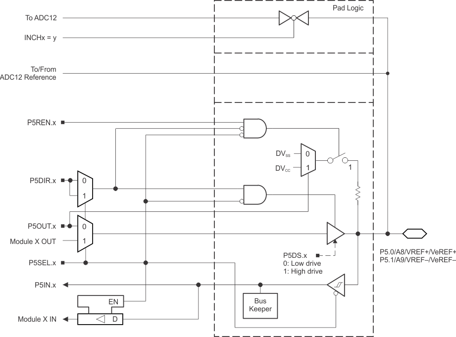
Table 8-46 Port P5 (P5.0 and P5.1) Pin Functions
| PIN NAME (P5.x) | x | FUNCTION | CONTROL BITS/SIGNALS (1) | ||
|---|---|---|---|---|---|
| P5DIR.x | P5SEL.x | REFOUT | |||
| P5.0/A8/VREF+/VeREF+ | 0 | P5.0 (I/O) (2) | I: 0; O: 1 | 0 | X |
| A8/VeREF+ (3) | X | 1 | 0 | ||
| A8/VREF+ (4) | X | 1 | 1 | ||
| P5.1/A9/VREF–/VeREF– | 1 | P5.1 (I/O) (2) | I: 0; O: 1 | 0 | X |
| A9/VeREF– (5) | X | 1 | 0 | ||
| A9/VREF– (6) | X | 1 | 1 | ||
(1) X = Don't care.
(2) Default condition.
(3) Setting the P5SEL.0 bit disables the output driver as well as the input Schmitt trigger to prevent parasitic cross currents
when applying analog signals. An external voltage can be applied to VeREF+ and used as the reference for the ADC12_A. Channel A8, when
selected with the INCHx bits, is connected to the VREF+/VeREF+ pin.
(4) Setting the P5SEL.0 bit disables the output driver as well as the input Schmitt trigger to prevent parasitic cross currents
when applying analog signals. The ADC12_A, VREF+ reference is available at the pin. Channel A8, when selected with the INCHx bits, is
connected to the VREF+/VeREF+ pin.
(5) Setting the P5SEL.1 bit disables the output driver as well as the input Schmitt trigger to prevent parasitic cross currents
when applying analog signals. An external voltage can be applied to VeREF- and used as the reference for the ADC12_A. Channel A9, when
selected with the INCHx bits, is connected to the VREF-/VeREF- pin.
(6) Setting the P5SEL.1 bit disables the output driver as well as the input Schmitt trigger to prevent parasitic cross currents
when applying analog signals. The ADC12_A, VREF– reference is available at the pin. Channel A9, when selected with the INCHx bits, is
connected to the VREF-/VeREF- pin.