JAJSDR3D September 2017 – December 2018 OPA2837 , OPA837
PRODUCTION DATA.
- 1 特長
- 2 アプリケーション
- 3 概要
- 4 改訂履歴
- 5 Pin Configuration and Functions
-
6 Specifications
- 6.1 Absolute Maximum Ratings
- 6.2 ESD Ratings
- 6.3 Recommended Operating Conditions
- 6.4 Thermal Information: OPA837
- 6.5 Thermal Information: OPA2837
- 6.6 Electrical Characteristics: VS = 5 V
- 6.7 Electrical Characteristics: VS = 3 V
- 6.8 Typical Characteristics: VS = 5.0 V
- 6.9 Typical Characteristics: VS = 3.0 V
- 6.10 Typical Characteristics: ±2.5-V to ±1.5-V Split Supply
- 7 Detailed Description
-
8 Application and Implementation
- 8.1
Application Information
- 8.1.1 Noninverting Amplifier
- 8.1.2 Inverting Amplifier
- 8.1.3 Output DC Error Calculations
- 8.1.4 Output Noise Calculations
- 8.1.5 Instrumentation Amplifier
- 8.1.6 Attenuators
- 8.1.7 Differential to Single-Ended Amplifier
- 8.1.8 Differential-to-Differential Amplifier
- 8.1.9 Pulse Application With Single-Supply Circuit
- 8.1.10 ADC Driver Performance
- 8.2 Typical Applications
- 8.1
Application Information
- 9 Power Supply Recommendations
- 10Layout
- 11デバイスおよびドキュメントのサポート
- 12メカニカル、パッケージ、および注文情報
パッケージ・オプション
メカニカル・データ(パッケージ|ピン)
サーマルパッド・メカニカル・データ
発注情報
8.2.1.3 Application Curves
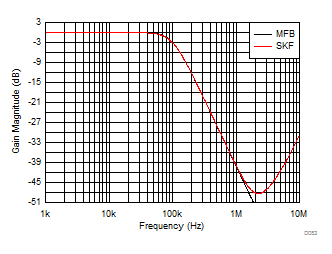
Figure 85 shows the comparative response curves for each of the filter design examples. Both filters hit the desired response shape exactly. However, notice the loss of stop-band rejection in the Sallen-Key design. This loss results from the op amp output impedance increasing at higher frequencies and allowing the signal to feed through the feedback capacitor to the output.
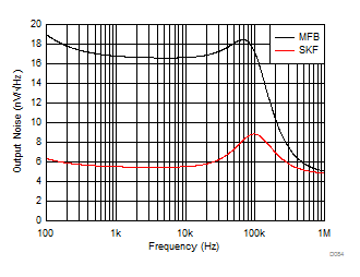
Figure 86 shows a comparison of the output spot noise for the two designs. The Sallen-Key is much lower because of the lower resistor values used. Also, the MFB shows a noise gain of 2 V/V versus the Sallen-Key gain of 1 V/V. This difference immediately increases the MFB output noise by at least twice the input voltage noise from the op amp. The higher resistor values also increase the total output noise for the MFB.

