JAJSFY9A December   2017  – August 2018 TLC6C5724-Q1

PRODUCTION DATA.  

  1. 特長
  2. アプリケーション
  3. 概要
    1.     代表的なアプリケーションの回路図
  4. 改訂履歴
  5. Pin Configuration and Functions
    1.     Pin Functions
  6. Specifications
    1. 6.1 Absolute Maximum Ratings
    2. 6.2 ESD Ratings
    3. 6.3 Recommended Operating Conditions
    4. 6.4 Thermal Information
    5. 6.5 Electrical Characteristics
    6. 6.6 Timing Requirements
    7. 6.7 Switching Characteristics
    8. 6.8 Typical Characteristics
  7. Detailed Description
    1. 7.1 Overview
    2. 7.2 Functional Block Diagram
    3. 7.3 Feature Description
      1. 7.3.1 Maximum Constant-Sink-Current Setting
      2. 7.3.2 Brightness Control and Dot Correction
      3. 7.3.3 Grayscale Configuration
        1. 7.3.3.1 PWM Auto Repeat
        2. 7.3.3.2 PWM Timing Reset
      4. 7.3.4 Diagnostics
        1. 7.3.4.1  LED Diagnostics
        2. 7.3.4.2  Adjacent-Pin-Short Check
        3. 7.3.4.3  IREF Short and IREF Open Detection
        4. 7.3.4.4  Pre-Thermal Warning Flag
        5. 7.3.4.5  Thermal Error Flag
        6. 7.3.4.6  Negate Bit Toggle
        7. 7.3.4.7  LOD_LSD Self-Test
        8. 7.3.4.8  ERR Pin
        9. 7.3.4.9  ERROR Clear
        10. 7.3.4.10 Global Reset
        11. 7.3.4.11 Slew Rate Control
        12. 7.3.4.12 Channel Group Delay
    4. 7.4 Device Functional Modes
      1. 7.4.1 Power Up
      2. 7.4.2 Device Initialization
      3. 7.4.3 Fault Mode
      4. 7.4.4 Normal Operation
    5. 7.5 Programming
      1. 7.5.1 Register Write and Read
        1. 7.5.1.1 FC-BC-DC Write
          1. 7.5.1.1.1 FC Data Write
          2. 7.5.1.1.2 BC Data Write
          3. 7.5.1.1.3 DC Data Write
        2. 7.5.1.2 Grayscale Data Write
        3. 7.5.1.3 Special Command Function
          1. 7.5.1.3.1 GS Read
          2. 7.5.1.3.2 FC-BC-DC Read
          3. 7.5.1.3.3 Status Information Data Read
    6. 7.6 Register Maps
      1. 7.6.1 GRAYSCALE Registers
        1. 7.6.1.1 OUTn_GS Register (Offset = 0h)
          1. Table 25. OUTn_GS Register Field Descriptions
      2. 7.6.2 FC-BC-DC Registers
        1. 7.6.2.1 FC-BC-DC Register (Offset = 1h)
          1. Table 28. FC-BC-DC Register Field Descriptions
      3. 7.6.3 SID Registers
        1. 7.6.3.1 SID Register (Offset = 2h)
          1. Table 31. SID Register Field Descriptions
  8. Application and Implementation
    1. 8.1 Application Information
    2. 8.2 Typical Application
      1. 8.2.1 Design Requirements
      2. 8.2.2 Detailed Design Procedure
      3. 8.2.3 Application Curves
  9. Power Supply Recommendations
  10. 10Layout
    1. 10.1 Layout Guidelines
    2. 10.2 Layout Example
  11. 11デバイスおよびドキュメントのサポート
    1. 11.1 ドキュメントの更新通知を受け取る方法
    2. 11.2 コミュニティ・リソース
    3. 11.3 商標
    4. 11.4 静電気放電に関する注意事項
    5. 11.5 Glossary
  12. 12メカニカル、パッケージ、および注文情報

パッケージ・オプション

メカニカル・データ(パッケージ|ピン)
サーマルパッド・メカニカル・データ
発注情報

ERR Pin

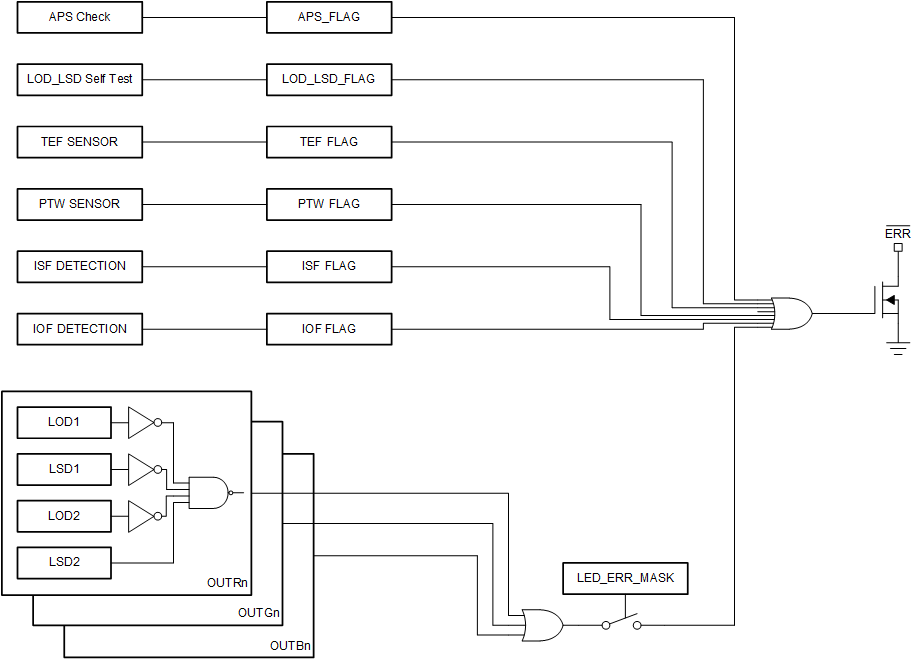
The TLC6C5724-Q1 device supports an active-low open-drain error output. Figure 24 shows the error pulldown block diagram. 10-bit error status information controls the error pulldown circuit directly. But LED failure can be masked by the LED_ERR_MASK bit. The LED_ERR_MASK value is 1 by default, so an LED failure is masked from the error pulldown circuit. Even if there is an LED failure, the ERR pin is not pulled down by this LED failure. If LED_ERR_MASK is 0, the ERR pin is pulled down by an LED failure to indicate an error scenario. Users can use an MCU interrupt to read out the fault information.
TLC6C5724-Q1 Error-Output-slasek2.gifFigure 24. ERR Pin Pulldown Scheme