JAJSKW6 december 2020 TMUXHS4412
PRODUCTION DATA
- 1
- 1 特長
- 2 アプリケーション
- 3 概要
- 4 Revision History
- 5 Pin Configuration and Functions
- 6 Specifications
- 7 Detailed Description
- 8 Application and Implementation
- 9 Power Supply Recommendations
- 10Layout
- 11Device and Documentation Support
- 12Mechanical, Packaging, and Orderable Information
パッケージ・オプション
メカニカル・データ(パッケージ|ピン)
- RUA|42
サーマルパッド・メカニカル・データ
- RUA|42
発注情報
8.2.1 PCIe Lane Muxing
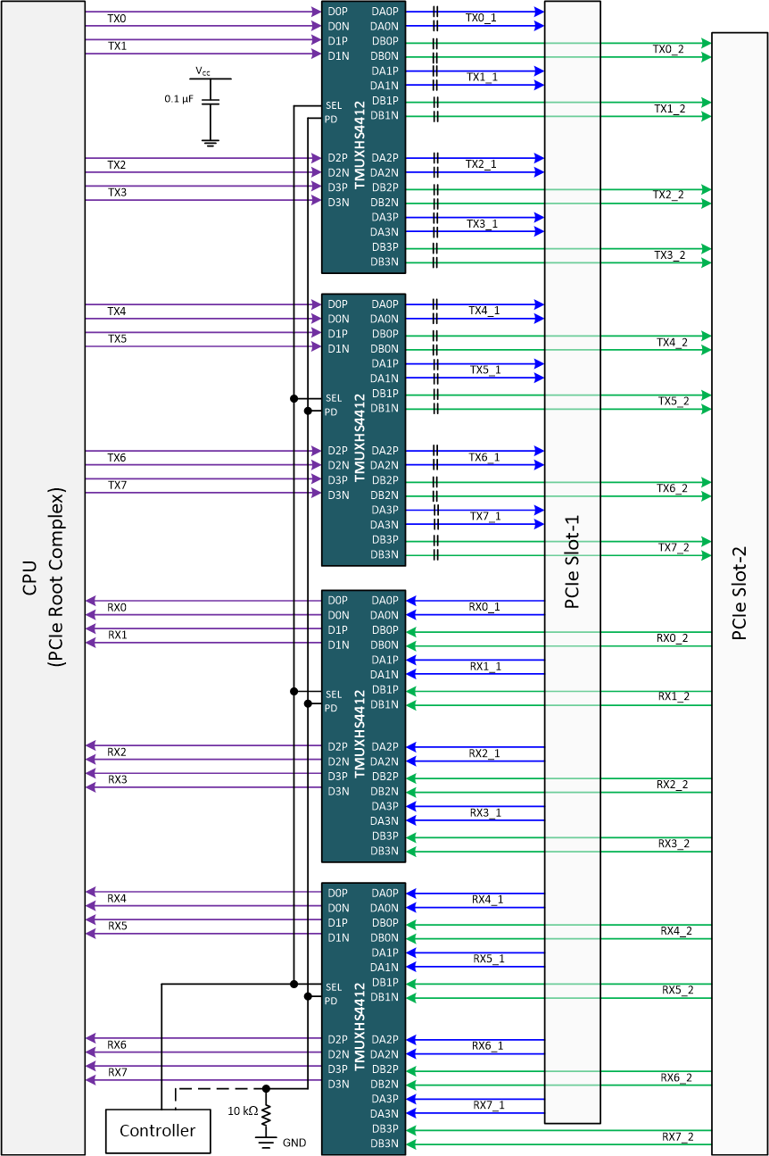
The TMUXHS4412 can be used to switch PCIe lanes between two slots. In many PC and server motherboards, the CPU does not have enough PCIe lanes to provide desired system flexibility for end customers. In such applications, the TMUXHS4412 can be used to switch PCIe TX and RX lanes between two slots. Figure 8-2 provides a schematic where four TMUXHS4412 are used to switch eight PCIe lanes (8-TX and 8-RX channels). Note the common mode voltage (CMV) bias for the TMUXHS4412 must be within the valid range. In implementations where receiver CMV bias of a PCIe root complex or an end point can not be ensured within the CMV range, additional DC blocking capacitors and appropriate CMV biasing must be implemented. One side of the device has AC coupling capacitors. Additionally the PD pin must be low for device to work. This pin can be driven by a processor.
 Figure 8-2 PCIe Lane Muxing