SLVSCH2 July 2014 TPS2105-EP
PRODUCTION DATA.
- 1 Features
- 2 Applications
- 3 Description
- 4 Revision History
- 5 Pin Configuration and Functions
- 6 Specifications
- 7 Detailed Description
- 8 Application and Implementation
- 9 Power Supply Recommendations
- 10Layout
- 11Device and Documentation Support
- 12Mechanical, Packaging, and Orderable Information
10 Layout
10.1 Layout Guidelines
- The IN1 and OUT pins of the TPS2105-EP can carry up to 500 mA, so trace to these pins should have short length and wider traces to minimize the voltage drop to the load.
- Both the IN1 and IN2 pins should be bypassed to ground with a low-ESR ceramic bypass capacitor. The typical recommended bypass capacitance is 0.22-µF ceramic capacitor.
- A bypass capacitor and a load capacitor are needed on the output terminal.
- TI recommends a 220-µF output load capacitor for 100-mA loads.
- Locating the 1-µF ceramic bypass capacitor at the output can improve the immunity of the device to short-circuit transients.
- The GND terminal should be tied to the PCB ground plane at the terminal of the DUT.
10.2 Layout Examples
 Figure 20. Input and Output Capacitors and DUT Area
 Figure 21. Enable, Input, Output, and Ground Pins
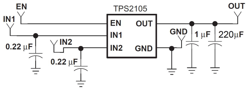 Figure 22. Schematics Diagram
Table 2. Component Descriptions
| PART | DESCRIPTION |
|---|---|
| C1, C2 | 0.22 µF, size 0805 |
| C3 | 1 µF, size 0805 |
| C4 | 220 µF, tantalum capacitors |
| U1 | TPS2105MDBVREP |
| TP_EN, TP_IN1, TP_IN2, TP_OUT, TP_GND | Test point, through hole |