SLVSCH2 July 2014 TPS2105-EP
PRODUCTION DATA.
- 1 Features
- 2 Applications
- 3 Description
- 4 Revision History
- 5 Pin Configuration and Functions
- 6 Specifications
- 7 Detailed Description
- 8 Application and Implementation
- 9 Power Supply Recommendations
- 10Layout
- 11Device and Documentation Support
- 12Mechanical, Packaging, and Orderable Information
6 Specifications
6.1 Absolute Maximum Ratings
over operating free-air temperature range (unless otherwise noted)(1)| MIN | MAX | UNIT | ||
|---|---|---|---|---|
| VI(IN1) | Input voltage(2) | –0.3 | 6 | V |
| VI(IN2) | Input voltage(2) | –0.3 | 6 | V |
| Input voltage, VI at EN(2) | –0.3 | 6 | V | |
| VO | Output voltage(2) | –0.3 | 6 | V |
| IO(IN1) | Continuous output current | 700 | mA | |
| IO(IN2) | Continuous output current | 140 | mA | |
| Continuous total power dissipation | See Thermal Information | |||
| TJ | Operating virtual junction temperature | –55 | 150 | °C |
| Lead temperature soldering 1.6 mm (1/16 inch) from case for 10 s | 260 | °C | ||
(1) Stresses beyond those listed under Absolute Maximum Ratings may cause permanent damage to the device. These are stress ratings only, and functional operation of the device at these or any other conditions beyond those indicated under Recommended Operating Conditions is not implied. Exposure to absolute-maximum-rated conditions for extended periods may affect device reliability.
(2) All voltages are with respect to GND.
6.2 Handling Ratings
| MIN | MAX | UNIT | |||
|---|---|---|---|---|---|
| Tstg | Storage temperature range | –65 | 150 | °C | |
| V(ESD) | Electrostatic discharge | Human body model (HBM), per ANSI/ESDA/JEDEC JS-001, all pins(1) | –2000 | 2000 | V |
| Machine model (MM) ESD stress voltage | –200 | 200 | |||
| Charged device model (CDM), per JEDEC specification JESD22-C101, all pins(2) | –750 | 750 | |||
(1) JEDEC document JEP155 states that 500-V HBM allows safe manufacturing with a standard ESD control process.
(2) JEDEC document JEP157 states that 250-V CDM allows safe manufacturing with a standard ESD control process.
6.3 Recommended Operating Conditions
over operating free-air temperature range (unless otherwise noted)| MIN | MAX | UNIT | ||
|---|---|---|---|---|
| VI(INx) | Input voltage | 2.7 | 5.5 | V |
| Input voltage, VI at EN | 0 | 5.5 | V | |
| IO(IN1) | Continuous output current | 500 | mA | |
| IO(IN2) | Continuous output current | 100(1) | mA | |
| TJ | Operating virtual junction temperature | –55 | 125 | °C |
(1) The device can deliver up to 220 mA at IO(IN2). However, operation at the higher current levels results in greater voltage drop across the device, and greater voltage droop when switching between IN1 and IN2.
6.4 Thermal Information
| THERMAL METRIC(1) | TPS2105-EP | UNIT | |
|---|---|---|---|
| DBV (5 PINS) | |||
| RθJA | Junction-to-ambient thermal resistance | 208.7 | °C/W |
| RθJC(top) | Junction-to-case (top) thermal resistance | 122.9 | |
| RθJB | Junction-to-board thermal resistance | 36.7 | |
| ψJT | Junction-to-top characterization parameter | 14.2 | |
| ψJB | Junction-to-board characterization parameter | 35.8 | |
| RθJC(bot) | Junction-to-case (bottom) thermal resistance | N/A | |
(1) For more information about traditional and new thermal metrics, see the IC Package Thermal Metrics application report, SPRA953.
6.5 Electrical Characteristics
Over recommended operating range (unless otherwise specified)| PARAMETER | TEST CONDITIONS | MIN | TYP | MAX | UNIT | |||
|---|---|---|---|---|---|---|---|---|
| POWER SWITCH | ||||||||
| rDS(on) | On-state resistance | IN1-OUT, VI(IN1) = 5.5 V, VI(IN2) = 0 V | 250 | 435 | mΩ | |||
| IN2-OUT, VI(IN2) = 5.5 V, VI(IN1) = 0 V | 1.3 | 2.4 | Ω | |||||
| ENABLE INPUT | ||||||||
| VIH | High-level input voltage | 2.7 V ≤ VI(INx) ≤ 5.5 V | 2 | V | ||||
| VIL | Low-level input voltage | 2.7 V ≤ VI(INx) ≤ 5.5 V | 0.8 | V | ||||
| II | Input current | EN = 0 V or EN = VI(INx) | –0.65 | 0.65 | µA | |||
| SUPPLY CURRENT | ||||||||
| II | Supply current | EN = L, IN2 selected | 0.75 | 1.5 | µA | |||
| EN = H, IN1 selected | 18 | 35 | µA | |||||

1. Wirebond life = Time at temperature with or without bias
2. Electromigration fail mode = Time at temperature with bias
3. Silicon operating life design goal is 10 years at 105°C junction temperature (does not include package interconnect life).
4. The predicted operating lifetime versus junction temperature is based on reliability modeling and available qualification data.
Figure 1. Predicted Lifetime Derating Chart for TPS2105-EP
6.6 Switching Characteristics
TJ = 25°C, VI(IN1) = VI(IN2) = 5 V (unless otherwise noted)| PARAMETER | TEST CONDITIONS | MIN | TYP | MAX | UNIT | |||
|---|---|---|---|---|---|---|---|---|
| tr | Output rise time | IN1-OUT | VI(IN2) = 0 | CL = 1 µF, IL = 500 mA | 340 | µs | ||
| CL = 10 µF, IL = 500 mA | 340 | |||||||
| CL = 1 µF, IL = 100 mA | 312 | |||||||
| IN2-OUT | VI(IN1) = 0 | CL = 1 µF, IL = 100 mA | 3.4 | |||||
| CL = 10 µF, IL = 100 mA | 34 | |||||||
| CL = 1 µF, IL = 10 mA | 3.5 | |||||||
| tf | Output fall time | IN1-OUT | VI(IN2) = 0 | CL = 1 µF, IL = 500 mA | 6 | µs | ||
| CL = 10 µF, IL = 500 mA | 108 | |||||||
| CL = 1 µF, IL = 100 mA | 8 | |||||||
| IN2-OUT | VI(IN1) = 0 | CL = 1 µF, IL = 100 mA | 100 | |||||
| CL = 10 µF, IL = 100 mA | 990 | |||||||
| CL = 1 µF, IL = 10 mA | 1000 | |||||||
| tPLH | Propagation delay time, low-to-high output |
IN1-OUT | VI(IN2) = 0 | CL = 10 µF, IL = 100 mA | 55 | µs | ||
| IN2-OUT | VI(IN1) = 0 | 1 | ||||||
| tPHL | Propagation delay time, high-to-low output |
IN1-OUT | VI(IN2) = 0 | CL = 10 µF, IL = 100 mA | 1.5 | µs | ||
| IN2-OUT | VI(IN1) = 0 | 50 | ||||||
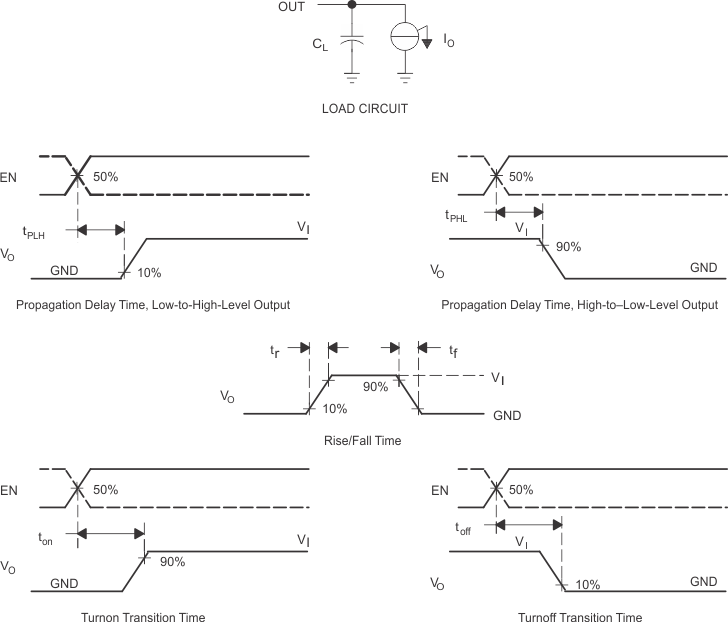 Figure 2. Test Circuit and Voltage Waveforms
6.7 Typical Characteristics

| VI(IN1) = 5 V | VI(IN2) = 0 V | TJ = 25°C |

| VI(IN1) = 5 V | VI(IN2) = 0 V | TJ = 25°C |

| VI(IN1) = 5 V | VI(IN2) = 5 V | TJ = 25°C |
| If switching from IN1 to IN2, the voltage droop is much smaller. | ||
| Thus, choose the load capacitance according to Figure 6. | ||

(IN1 Enabled)


| VI(IN1) = 0 V | VI(IN2) = 5 V | TJ = 25°C |

| VI(IN1) = 0 V | VI(IN2) = 5 V | TJ = 25°C |

| VI(IN1) = 5 V | VI(IN2) = 0 V | RL = 10 Ω |
| TJ = 25°C | ||

(IN1 Disabled)

