JAJSGC8B October 2018 – January 2020 TPS25982
PRODUCTION DATA.
- 1 特長
- 2 アプリケーション
- 3 概要
- 4 改訂履歴
- 5 デバイス比較表
- 6 概要 (続き)
- 7 Pin Configuration and Functions
- 8 Specifications
-
9 Detailed Description
- 9.1 Overview
- 9.2 Functional Block Diagram
- 9.3 Feature Description
- 9.4 Fault Response
- 9.5 Device Functional Modes
-
10Application and Implementation
- 10.1 Application Information
- 10.2
Typical Application: Standby Power Rail Protection in Datacenter Servers
- 10.2.1 Design Requirements
- 10.2.2
Detailed Design Procedure
- 10.2.2.1 Device Selection
- 10.2.2.2 Setting the Current Limit Threshold: RILIM Selection
- 10.2.2.3 Setting the Undervoltage Lockout Set Point
- 10.2.2.4 Choosing the Current Monitoring Resistor: RIMON
- 10.2.2.5 Setting the Output Voltage Ramp Time (TdVdt)
- 10.2.2.6 Setting the Load Handshake (LDSTRT) Delay
- 10.2.2.7 Setting the Transient Overcurrent Blanking Interval (tITIMER)
- 10.2.2.8 Setting the Auto-Retry Delay and Number of Retries
- 10.2.3 Application Curves
- 10.3 System Examples
- 11Power Supply Recommendations
- 12Layout
- 13デバイスおよびドキュメントのサポート
- 14メカニカル、パッケージ、および注文情報
パッケージ・オプション
メカニカル・データ(パッケージ|ピン)
- RGE|24
サーマルパッド・メカニカル・データ
- RGE|24
発注情報
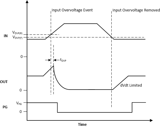
9.3.2 Overvoltage Protection (OVP)
The TPS25982 implements Overvoltage Lock-Out (OVLO) on IN to protect the output load in the event of input overvoltage. When the input exceeds the Overvoltage Protection threshold (VOVP(R)) the device turns off the output within tOVP. As long as an overvoltage condition is present on the input, the device stays disabled and the output will be turned off. Once the input voltage returns to the normal operating range, the device attempts to start up normally.
 Figure 43. Overvoltage Response
 There are multiple device options with different fixed overvoltage thresholds to choose from, including one without internal overvoltage protection. See the Device Comparison Table for a list of available options.