JAJSRN4A July 2023 – October 2023 TPS25984
PRODUCTION DATA
- 1
- 1 特長
- 2 アプリケーション
- 3 概要
- 4 Revision History
- 5 概要 (続き)
- 6 Pin Configuration and Functions
- 7 Specifications
-
8 Detailed Description
- 8.1 Overview
- 8.2 Functional Block Diagram
- 8.3
Feature Description
- 8.3.1 Undervoltage Protection
- 8.3.2 Insertion Delay
- 8.3.3 Overvoltage Protection
- 8.3.4 Inrush Current, Overcurrent, and Short-Circuit Protection
- 8.3.5 Analog Load Current Monitor (IMON)
- 8.3.6 Mode Selection (MODE)
- 8.3.7 Parallel Device Synchronization (SWEN)
- 8.3.8 Stacking Multiple eFuses for Unlimited Scalability
- 8.3.9 Analog Junction Temperature Monitor (TEMP)
- 8.3.10 Overtemperature Protection
- 8.3.11 Fault Response and Indication (FLT)
- 8.3.12 Power-Good Indication (PG)
- 8.3.13 Output Discharge
- 8.3.14 FET Health Monitoring
- 8.3.15 Single Point Failure Mitigation
- 8.4 Device Functional Modes
- 9 Application and Implementation
- 10Device and Documentation Support
- 11Mechanical, Packaging, and Orderable Information
8.3.4.2 Steady-State Overcurrent Protection (Circuit-Breaker)
The TPS25984x responds to output overcurrent conditions during steady-state by performing a circuit-breaker action after a user-adjustable transient fault blanking interval. This action allows the device to support a higher peak current for a short user-defined interval but also ensures robust protection in case of persistent output faults.
The device constantly senses the output load current and provides an analog current output (IIMON) on the IMON pin which is proportional to the load current, which in turn produces a proportional voltage (VIMON) across the IMON pin resistor (RIMON) as per Equation 4.
Where GIMON is the current monitor gain (IIMON : IOUT)
The overcurrent condition is detected by comparing this voltage against the voltage on the IREF pin as a reference. The reference voltage (VIREF) can be controlled in two ways, which sets the overcurrent protection threshold (IOCP) accordingly.
- In the standalone or primary mode of operation,
the internal current source interacts with the
external IREF pin resistor (RIREF) to
generate the reference voltage. It is also
possible to drive the IREF pin from an external
low impedance reference voltage source as shown in
Equation 5. Equation 5.
- In a primary and secondary parallel configuration, the primary eFuse or controller drives the voltage on the IREF pin to provide an external reference (VIREF) for all the secondary devices in the chain.
The overcurrent protection threshold during steady-state (IOCP) can be calculated using Equation 6.
Maintain VIREF within the recommended voltage range to ensure proper operation of the overcurrent detection circuit.
TI recommends to add a 150-pF capacitor from IREF pin to GND for improved noise immunity.
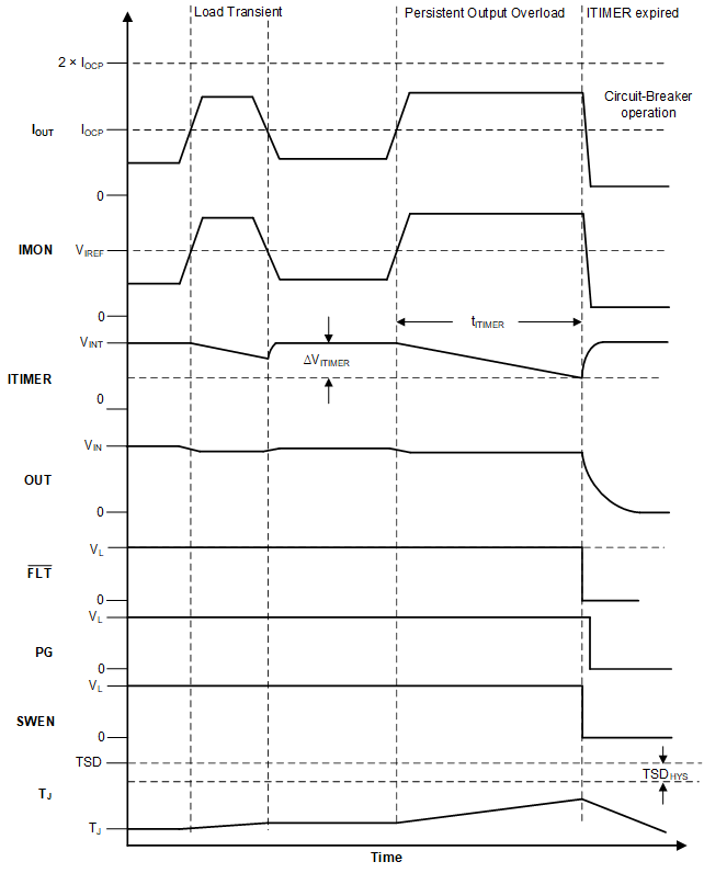
After an overcurrent condition is detected, that is the load current exceeds the programmed current limit threshold (IOCP), but stays lower than the short-circuit threshold (2 × IOCP), the device starts discharging the ITIMER pin capacitor using an internal 2-μA pulldown current. If the load current drops below the current limit threshold before the ITIMER capacitor discharges by ΔVITIMER, the ITIMER is reset by pulling it up to VINT internally and the circuit-breaker action is not engaged. This action allows short overload transient pulses to pass through the device without tripping the circuit. If the overcurrent condition persists, the ITIMER capacitor continues to discharge and after it falls by ΔVITIMER, the circuit-breaker action turns off the FET immediately. At the same time, the ITIMER cap is charged up to VINT again so that it is at its default state before the next overcurrent event. This action ensures the full blanking timer interval is provided for every overcurrent event. Equation 24 can be used to calculate the RIMON value for the desired overcurrent threshold.
The duration for which transients are allowed can be adjusted using an appropriate capacitor value from ITIMER pin to ground. The transient overcurrent blanking interval can be calculated using Equation 8.
Leave the ITIMER pin open to allow the part to break the circuit with the minimum possible delay. However, leaving the pin open makes the circuit-breaker response extremely sensitive to noise and can cause false tripping during load transients.
Shorting the ITIMER pin to ground results in minimum overcurrent response delay (similar to ITIMER pin open condition), but increases the quiescent current – not a recommended mode of operation.
Increasing the ITIMER cap value extends the overcurrent blanking interval. However, it also extends the time needed for the ITIMER cap to recharge up to VINT before the next overcurrent event. If the next overcurrent event occurs before the ITIMER cap is recharged fully, it takes less time to discharge to the VITIMER threshold, thereby it provides a shorter blanking interval than intended.
Figure 8-4 illustrates the overcurrent response for TPS25984x eFuse. After the part shuts down due to a circuit-breaker fault, it either stays latched off (TPS259840 variant) or restarts automatically after a fixed delay (TPS259841 variant).
 Figure 8-4 Steady-State Overcurrent (Circuit-Breaker) Response