SLVSBP4D December 2012 – September 2014 TPS43060 , TPS43061
PRODUCTION DATA.
- 1 Features
- 2 Applications
- 3 Description
- 4 Simplified Schematic
- 5 Revision History
- 6 Pin Configuration and Functions
- 7 Specifications
-
8 Detailed Description
- 8.1 Overview
- 8.2 Functional Block Diagram
- 8.3
Feature Description
- 8.3.1 Switching Frequency
- 8.3.2 Low-Dropout Regulator
- 8.3.3 Input Undervoltage (UV)
- 8.3.4 Enable and Adjustable UVLO
- 8.3.5 Voltage Reference and Setting Output Voltage
- 8.3.6 Minimum On-Time and Pulse Skipping
- 8.3.7 Zero-Cross Detection and Duty Cycle
- 8.3.8 Minimum Off-Time and Maximum Duty Cycle
- 8.3.9 Soft-Start
- 8.3.10 Power Good
- 8.3.11 Overvoltage Protection (OVP)
- 8.3.12 OVP and Current Sense Resistor Selection
- 8.3.13 Gate Drivers
- 8.3.14 Thermal Shutdown
- 8.4 Device Functional Modes
-
9 Application and Implementation
- 9.1 Application Information
- 9.2
Typical Applications
- 9.2.1
Synchronous Boost Converter Typical Application Using TPS43061
- 9.2.1.1 Design Requirements
- 9.2.1.2
Detailed Design Procedure
- 9.2.1.2.1 Selecting the Switching Frequency
- 9.2.1.2.2 Inductor Selection
- 9.2.1.2.3 Selecting the Current Sense Resistor
- 9.2.1.2.4 Output Capacitor Selection
- 9.2.1.2.5 MOSFET Selection - NexFET Power Block
- 9.2.1.2.6 Bootstrap Capacitor Selection
- 9.2.1.2.7 VCC Capacitor
- 9.2.1.2.8 Input Capacitor
- 9.2.1.2.9 Output Voltage and Feedback Resistors Selection
- 9.2.1.2.10 Setting the Soft-Start Time
- 9.2.1.2.11 UVLO Set Point
- 9.2.1.2.12 Power Good Resistor Selection
- 9.2.1.2.13 Control Loop Compensation
- 9.2.1.2.14 DCM, Pulse-Skip Mode, and No-Load Input Current
- 9.2.1.3 Application Curves
- 9.2.2 High-Efficiency 40-V Synchronous Boost Converter Typical Application Using TPS43060
- 9.2.1
Synchronous Boost Converter Typical Application Using TPS43061
- 10Power Supply Recommendations
- 11Layout
- 12Device and Documentation Support
- 13Mechanical, Packaging, and Orderable Information
パッケージ・オプション
メカニカル・データ(パッケージ|ピン)
- RTE|16
サーマルパッド・メカニカル・データ
- RTE|16
発注情報
9 Application and Implementation
NOTE
Information in the following applications sections is not part of the TI component specification, and TI does not warrant its accuracy or completeness. TI’s customers are responsible for determining suitability of components for their purposes. Customers should validate and test their design implementation to confirm system functionality.
9.1 Application Information
The TPS4306x device is a 4.5- to 38-V input, 58-V maximum output, step-up controller with integrated MOSFET drivers to create a synchronous boost power supply. This device is typically used to convert a lower DC voltage to a higher DC voltage. The maximum current is limited using an external resistor between the ISNS+ and ISNS– pins or the thermal performance of the external MOSFETs. Example applications are: 5, 12, and 24 V industrial, automotive and communications power systems, or battery-powered systems. Use the following design procedure to select component values for the TPS4306x device. This procedure illustrates the design of a high frequency switching regulator using ceramic output capacitors. Calculations can be done with the excel spreadsheet (SLVC471) located on the product page for TPS43060 and TPS43061. Alternately, use the WEBENCH® software to generate a complete design. The WEBENCH software uses an iterative design procedure and accesses a comprehensive database of components when generating a design. This section presents a simplified discussion of the design process.
9.2 Typical Applications
9.2.1 Synchronous Boost Converter Typical Application Using TPS43061
9.2.1.1 Design Requirements
The following section provides a step-by-step design guide of a high-frequency, high-power-density synchronous boost converter with the TPS43061 controller combined with a NexFET power block. This design procedure is also applicable to the TPS43060. The designer must know a few parameters to start the design process. These requirements are typically determined at the system level. For this example, start with the following known parameters.
Table 1. Key Parameters of the Boost Converter Example
| Parameter | Value |
|---|---|
| Input voltage (VIN) | 6 to 12.6 V, 9 V nominal |
| Output voltage (VOUT) | 15 V |
| Maximum output current (IOUT) | 2 A |
| Transient response to 0.5 A to 1.5 A load step (ΔVOUT) | 4% of VOUT = 0.6 V |
| Output voltage ripple (VRIPPLE) | 0.5% of VOUT = 0.075 V |
| Start input voltage (VSTART) | 5.34 V |
| Start input voltage (VSTOP) | 4.3 V |
9.2.1.2 Detailed Design Procedure
9.2.1.2.1 Selecting the Switching Frequency
The first step is to determine the switching frequency of the power converter. Be sure to consider the tradeoffs when selecting a higher or lower switching frequency. Typically, the designer uses the highest switching frequency possible because this results in the smallest solution size. A higher switching frequency allows for lower-value inductors and smaller-output capacitors compared to a power converter that switches at a lower frequency. A lower switching frequency produces a larger solution size, but typically has better efficiency. Setting the frequency for the minimum tolerable efficiency produces the optimum solution size for the application.
The switching frequency can also be limited by the minimum on-time and off-time of the controller based on the input voltage and the output voltage of the application. To determine the maximum allowable switching frequency, first estimate the CCM duty cycle using Equation 11 with the minimum and maximum input voltages. Equation 12 and Equation 13 should then be used to calculate the upper limit of switching frequency for the regulator. Choose the lower value result from these two equations. Switching frequencies higher than the calculated values result in either pulse skipping if the minimum on-time restricts the duty cycle or insufficient boost output voltage if the PWM duty cycle is limited by the minimum off-time.


The typical minimum on-time and off-time of the device are 100 ns and 250 ns, respectively. For this design, the duty cycle is estimated at 20% and 60% with the maximum input voltage and minimum input voltage, respectively. When operating at switching frequencies less than 200 kHz, the minimum off-time starts to increase and is equal to 5% of the switching period. 1.6 MHz is the estimated allowed maximum switching frequency based on Equation 12 and Equation 13 . When operating near the estimated maximum duty cycle, more accurate estimations of the duty cycle should be made by including the voltage drops of the external MOSFETs, sense resistor, and DCR of the inductor.
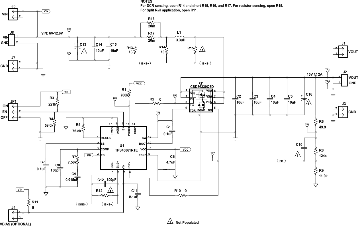
A switching frequency of 750 kHz was chosen as a compromise between efficiency and small solution size. To determine the timing resistance for a given switching frequency, use either Equation 14 or the curve in Figure 17. The switching frequency is set by resistor R5, shown in the schematic in Synchronous Boost Converter Typical Application Using TPS43061. For 750-kHz operation, the closest standard value resistor is 76.8 kΩ.

9.2.1.2.2 Inductor Selection
The selection of the inductor affects the steady-state operation as well as transient behavior and loop stability. These factors make it an important component in a switching power-supply design. The three most important inductor specifications to consider are inductor value, DC resistance (DCR), and saturation current rating. Let the parameter KIND represent the ratio of inductor peak-to-peak ripple current to the average inductor current. In a boost topology, the average inductor current is equal to the input current. The current delivered to the output is the input current modulated at the duty cycle of the PWM. The inductor ripple current contributes to the output current ripple that must be filtered by the output capacitor. Therefore, choosing high inductor ripple currents impacts the selection of the output capacitor. The value of KIND in the design using low-ESR output capacitors, such as ceramics, can be relatively higher than that in the design using higher-ESR output capacitors. Higher values of KIND lead to DCM operation at moderate to light loads.
To calculate the minimum value of the output inductor, use Equation 16 or Equation 17. In a boost topology, maximum current ripple occurs at 50% duty cycle. Use Equation 16 if the design will operate with 50% duty cycle. If not, use Equation 17. In Equation 17, use the input voltage value that is nearest to 50% duty-cycle operation.
For this design example, Equation 15 produces the estimated maximum input current (IIN) of 5 A. In reality, IIN will be higher because the simplified equations do not include the efficiency losses of the power supply. Using KIND = 0.3 with Equation 16, the minimum inductor value is calculated to be 3.33 µH. The nearest standard value of 3.3 µH is chosen. It is important that the RMS current and saturation current ratings of the inductor are not exceeded. The RMS and peak inductor current can be found from Equation 18 and Equation 19, respectively. The calculated RMS inductor current is 5 A, and the peak inductor current is 5.73 A. The chosen inductor is a Vishay IHLP2525CZER3R3M1, which has an RMS current rating of 6 A, a saturation current rating of 10 A, and 30-mΩ DCR.


Selecting higher ripple currents increases the output voltage ripple of the regulator, but allows for a lower inductance value.
The current flowing through the inductor is the inductor ripple current plus the average input current. During power-up, load faults, or transient load conditions, the inductor current can increase above the peak inductor current calculated previously. The prior equations also do not include the efficiency of the regulator. For this reason, a more conservative design approach is to choose an inductor with a saturation current rating greater than the typical switch current limit set by the current sense resistor or the inductor DC resistance if lossless DCR sensing is used.
9.2.1.2.3 Selecting the Current Sense Resistor
The external current sense resistor sets the cycle-by-cycle peak current limit. The peak current limit should be set to assure the maximum load current can be supported at the minimum input voltage. The typical overcurrent threshold voltage (VCS) with respect to duty cycle is shown in Figure 20. In this design example, the typical current limit threshold voltage at the 60% maximum duty cycle is 68 mV.
When selecting the current limit for the design, TI recommends a 20% margin from the calculated peak current limit in Equation 19 to allow for load and line transients and the efficiency loss of the design. Calculate the recommended current sense resistance with Figure 20. In this example, the minimum resistance is calculated at 9.89 mΩ and two 20-mΩ resistors in parallel are used. The sense resistors must be rated for the power dissipation calculated in Equation 22. Using the maximum current limit threshold of 82 mV according to the electrical specification table, the maximum power loss in the current sense resistor is 0.672 W. Two 0.5-W rated sense resistors are used in parallel in this design.


The 10-Ω series resistors, R13 and R15, with the 100-pF capacitor C12 filter high-frequency switching noise from the ISNS pins.
9.2.1.2.4 Output Capacitor Selection
In a boost topology, the current supplied to the output capacitor is discontinuous and proper selection of the output capacitor is important for filtering the high di/dt path of the supply. The designer must account for two primary considerations for selecting the value of the output capacitor. The output capacitor determines the output voltage ripple and how the supply responds to a large change in load current. The output capacitance must be selected based on the more stringent of these two criteria.
The first criterion is the desired response to a large change in load current. A PWM controller cannot immediately respond to a fast increase or decrease in the load current. The response time is determined by the loop bandwidth. The output capacitor must supply the increased load current or absorb the excess inductor current until the controller responds. Equation 23 estimates the minimum output capacitance needed for the desired ΔVOUT for a given ΔIOUT. The loop bandwidth (ƒBW) is typically limited by the right-half-plane zero (RHPZ) of the boost topology. The maximum recommended bandwidth can be calculated from Equation 41 and Equation 42. See the compensation section for more information. In this example, to limit the voltage deviation to 600 mV from a 1-A load step with a 14.5-kHz maximum bandwidth, a minimum of 18.3-µF output capacitance is needed. This value does not take into account the ESR of the output capacitor, which can typically be ignored when using ceramic capacitors.
The output capacitor absorbs the ripple current through the synchronous switch to limit the output voltage ripple. Equation 24 calculates the minimum output capacitance needed to meet the output voltage ripple specification. In this example, a minimum of 21.3 µF is needed. Again, this value does not take into account the ESR of the output capacitor.


The most stringent criterion for the output capacitor is 21.3 µF required to limit the output voltage ripple. When using ceramic capacitors for switching power supplies, TI recommends high-quality type X5R or X7R. They have a high capacitance-to-volume ratio and are fairly stable over temperature. Capacitance deratings for aging, temperature, and dc bias increase the minimum value required. The voltage rating must be greater than the output voltage with some tolerance for output voltage ripple and overshoot in transient conditions. For this example, 4 × 10-µF, 25-V ceramic capacitors with 5 mΩ of ESR are used. The estimated derated capacitance is 22 µF, approximately equal to the calculated minimum.
9.2.1.2.5 MOSFET Selection – NexFET Power Block
The TPS43061 5.5-V gate drive is optimized for low Qg NexFET power devices. NexFET power blocks with both the high-side and low-side MOSFETs integrated are ideal for high-power-density designs. This design example uses the CSD86330Q3D. Two primary considerations when selecting the power MOSFETs are the average gate drive current required and the estimated MOSFET power losses.
The average gate drive current must be less than the 50-mA (minimum) VCC supply current limit. This current is calculated using Equation 25. With the selected power block and 5.5-V VCC, the low-side FET has a total gate charge of 11 nC and the high-side FET has a total gate charge of 5 nC. The required gate drive current is 12 mA.

The target efficiency of the design dictates the acceptable power loss in the MOSFETs. The two largest components of power loss in the low-side FET are switching and conduction losses. Both losses are highest at the minimum input voltage when low-side FET current is maximum. The conduction power loss in the low-side FET can be calculated with Equation 26. Switching losses occur during the turn-off and turn-on time of the MOSFET. During these transitions, the low-side FET experiences both the input current and output voltage. The switching loss can be estimated with Equation 27. The low-side FET of the CSD86330Q3D has RDS(on)LS = 4.2 mΩ, gate-to-drain charge Qgd = 1.6 nC, output capacitance COSS = 680 pF, series gate resistance RG = 1.2 Ω, and gate-to-source voltage threshold VGS(th) = 1.1 V. The conduction power losses are estimated at 0.042 W and the switching losses are estimated at 0.070 W.


Two power losses in the high-side FET to consider are the dead time body diode loss and the FET conduction loss. The conduction loss is highest at the minimum PWM duty cycle. The conduction power loss in the high-side FET can be calculated with Equation 28. Dead time losses are caused by conduction in the body diode of the high-side FET during the delay time between the LDRV and HDRV signals. The dead time loss varies mainly with switching frequency. The dead time losses are estimated with Equation 29. The high-side FET of the CSD86330Q3D has RDS(ON)HS = 8 mΩ and body diode forward voltage drop VSD = 0.75 V. The conduction power losses are estimated at 0.080 W and the dead time losses are estimated at 0.366 W. For designs targeting highest efficiency, dead time losses can be reduced by adding a Schottky diode in parallel with the high-side FET to reduce the diode forward voltage drop during the dead time.


9.2.1.2.6 Bootstrap Capacitor Selection
A capacitor must be connected between the BOOT and SW pins for proper operation. This capacitor provides the instantaneous charge and gate drive voltage needed to turn on the high-side FET. TI recommends a ceramic with X5R or better grade dielectric. Use Equation 30 to calculate the minimum bootstrap capacitance to limit the BOOT capacitor ripple voltage to 250 mV. In this example with the selected high-side FET, the minimum calculated capacitance is 0.042 µF and a 0.1-µF capacitor is used. The capacitor should have a 10-V or higher voltage rating.

9.2.1.2.7 VCC Capacitor
An X5R or better grade ceramic bypass capacitor is required for the internal VCC regulator at the VCC pin with a recommended range of 0.47 to 10 µF. This example uses a capacitance of 4.7 µF. The capacitor should have a 10-V or higher voltage rating.
9.2.1.2.8 Input Capacitor
The TPS4306x requires a high-quality 0.1 µF or higher ceramic-type X5R or X7R bypass capacitor at the VIN pin for proper decoupling. Based on the application requirements, additional bulk capacitance may be needed to meet input voltage ripple and/or transient requirements. The minimum capacitance for a specified input voltage ripple is calculated using Equation 31. The voltage rating of the input capacitor must be greater than the maximum input voltage. The capacitor must also have a ripple current rating greater than the RMS current calculated with Equation 32. If ceramic input capacitors are used, they should be a high-quality ceramic, type X5R or X7R.
For this example design, the capacitors must be rated for at least 12 V to support the maximum input voltage. Designing for a 45-mV input voltage ripple (0.5% the nominal input voltage), the minimum input capacitance is 10.8 µF. The input capacitor must also be rated for 0.42 A RMS current. The capacitors selected are 2 × 10-µF, 25-V ceramic capacitors with 5 mΩ of ESR. The estimated voltage derated total capacitance is 15 µF.


9.2.1.2.9 Output Voltage and Feedback Resistors Selection
The voltage divider of R8 and R9 sets the output voltage. To balance power dissipation and noise sensitivity, R9 should be selected between 10 and 100 kΩ. For the example design, 11 kΩ was selected for R9. Using Equation 33, R8 is calculated as 124.2 kΩ. The nearest standard 1% resistor 124 kΩ is used.

where
- RLS = R9
- RHS = R8
9.2.1.2.10 Setting the Soft-Start Time
The soft-start capacitor determines the amount of time allowed for the output voltage to reach its nominal programmed value during power-up. This is especially useful if a load requires a controlled voltage slew rate. A controlled start-up time is necessary with large output capacitance to limit the current into the capacitor during start-up. Large input currents charging the output capacitors during start-up could trigger the current limit. Excessive current draw from the input power supply may also cause the input voltage rail to sag. The soft-start capacitor can be sized to limit in-rush current or output voltage overshoot during startup. Use Equation 34 to calculate the required capacitor for a desired soft-start time. In this example application for a desired soft-start time of 20 ms, a 0.082-µF capacitance is calculated, and the nearest standard value of 0.1-µF capacitor is chosen.

9.2.1.2.11 UVLO Set Point
The UVLO can be adjusted using an external voltage divider connected to the EN pin of the TPS4306x. The UVLO has two thresholds, one for power-up when the input voltage is rising and one for power-down or brown outs when the input voltage is falling. The necessary voltage divider resistors are calculated with Equation 35 and Equation 36. If the application does not require an adjustable UVLO, the EN pin can be left floating or tied to the VIN pin.
For the example design, the supply should start switching when the input voltage increases to 5.34 V (VSTART). After start-up, it should continue to operate until the input voltage falls to 4.3 V (VSTOP). To produce the desired start and stop voltages, this example uses resistor divider values R3 = 221 kΩ between VIN and EN and a R4 = 59 kΩ between EN and GND.


9.2.1.2.12 Power Good Resistor Selection
The PGOOD pin is an open-drain output requiring a pullup resistor connected to a voltage supply of no more than 8 V. TI recommends a value between 10 and 100 kΩ. If the Power Good indicator feature is not needed, this pin can be grounded or left floating.
9.2.1.2.13 Control Loop Compensation
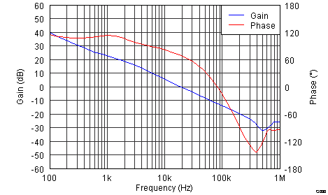
There are several methods to design compensation for DC-DC regulators. The method presented here is easy to calculate and ignores the effects of the slope compensation internal to the device. Because the slope compensation is ignored, the actual crossover frequency will be lower than the crossover frequency used in the calculations. This method assumes the crossover frequency is between the modulator pole and ESR zero of the output capacitor. In this simplified model, the DC gain (Adc), modulator pole (ƒPmod), and the ESR zero (ƒZmod) are calculated with Equation 37 to Equation 39. Use the derated value of COUT, which is 22 µF in this example. In a boost topology, the maximum crossover frequency is typically limited by the RHPZ. The RHPZ can be estimated with Equation 40. The compensation design should be done at the minimum input voltage when the RHPZ is at the lowest frequency. The crossover frequency should also be limited to less than 1/5 of the switching frequency. Equation 41 and Equation 42 are used to calculate the maximum recommended crossover frequency. For this example design, Adc = 11.3 V/V, ƒPmod = 0.97 kHz, ƒZmod = 1.45 MHz, ƒRHPZ = 57.9 kHz, ƒco1 = 14.5 kHz, and ƒco2 = 150 kHz. The target ƒco is 14.5 kHz.


The compensation components can now be calculated. A resistor in series with a capacitor creates a compensating zero. A capacitor in parallel to these two components can be added to form a compensating pole. Use Equation 43 to determine the compensation resistor (R7). R7 is calculated to be 7.45 kΩ and a standard 1% value of 7.5 kΩ is selected. Use Equation 44 to set the compensation zero to 1/10 the target crossover frequency. C9 is calculated at 0.0147 µF and a standard value of 0.015 µF is used.


A compensation pole can be implemented, if desired, with capacitor C8 in parallel with the series combination of R7 and C9. Use the larger value calculated from Equation 45 and Equation 46. The selected value of C8 is 150 pF for this example.


9.2.1.2.14 DCM, Pulse-Skip Mode, and No-Load Input Current
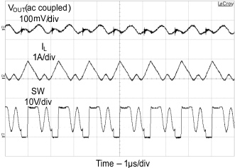
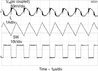
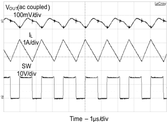
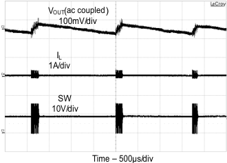
The reverse current sensing of the TPS4306x allows the power supply to operate in DCM at light loads for higher efficiency. The supply enters DCM when the inductor current ramps to 0 at the end of a PWM cycle and the reverse current sense turns off the high-side FET for the remainder of the cycle. In DCM, the duty cycle is a function of the load, input and output voltages, inductance, and switching frequency as computed in Equation 47. The load current at which the inductor current falls to 0 and the converter enters DCM can be calculated using Equation 48. Additionally, after the converter enters DCM, decreasing the load further reduces the duty cycle. If the DCM on-time reaches the minimum on-time of the TPS4306x, the converter begins pulse skipping to maintain output voltage regulation. Pulse skipping can increase the output voltage ripple.
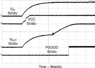
In this example with the 9-V nominal input voltage, the estimated load current where the converter enters DCM operation is 0.44 A. The measured boundary is 0.36 A. In most designs, the converter enters DCM at lower load currents because Equation 48 does not account for the efficiency losses. The design example power supply enters pulse-skip mode when the output current is lower than 12 mA and the input current draw is 1.3 mA with no load.


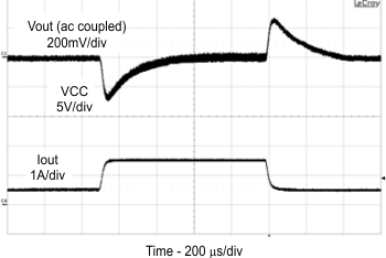
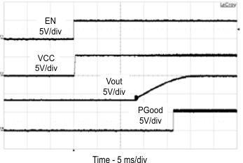
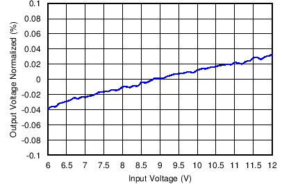
9.2.1.3 Application Curves

9.2.2 High-Efficiency 40-V Synchronous Boost Converter Typical Application Using TPS43060
9.2.2.1 Design Requirements
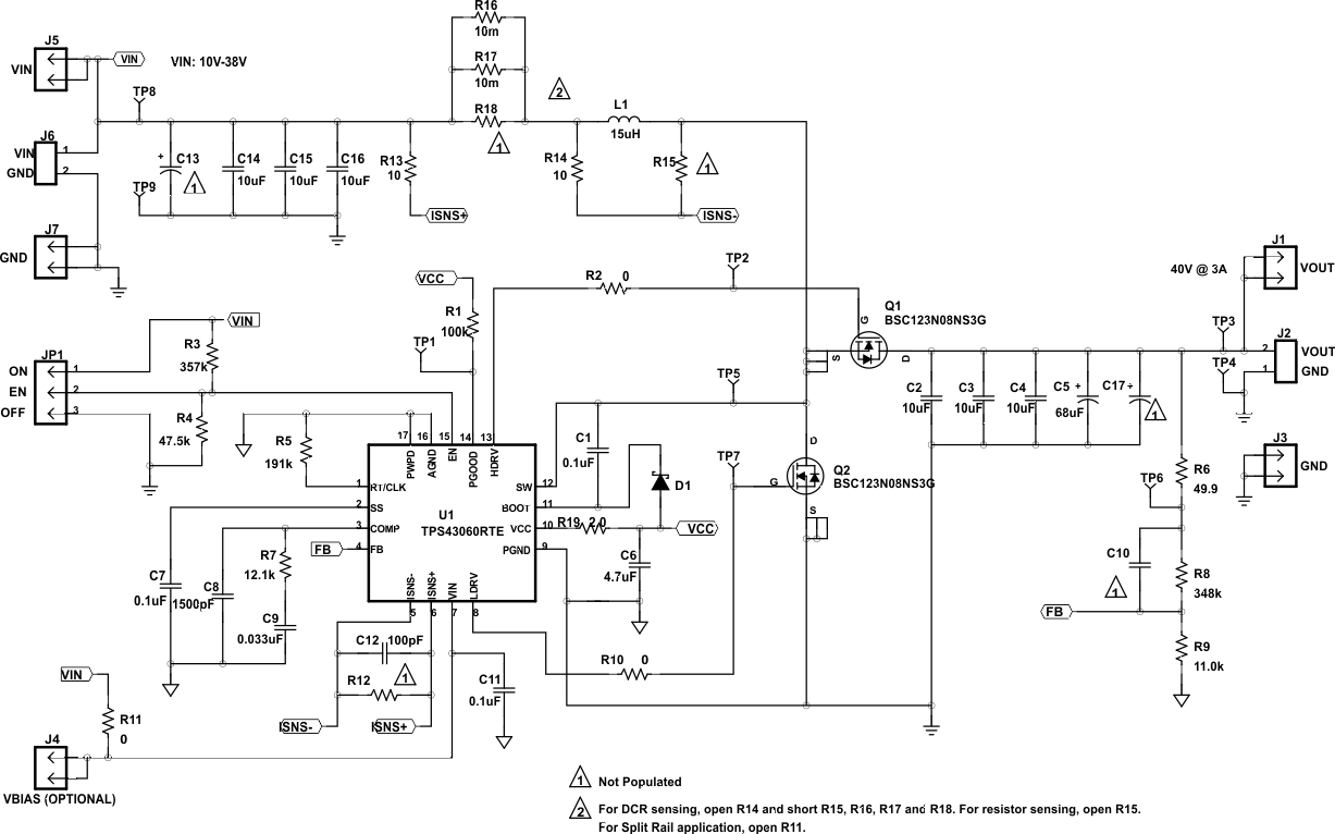
The design requirements and procedure of TPS43061 is also applicable to the TPS43060; however, several differences should be noted. Unlike the TPS43061, which has a 5.5-V gate drive supply and is optimized for low Qg NexFETs, the TPS43060 has a 7.5-V gate drive supply and is suitable to drive standard threshold MOSFETs. The TPS43060 requires an external bootstrap diode (D1 as shown in Figure 34) from VCC to BOOT to charge the bootstrap capacitor, and the external diode should have a breakdown voltage rating greater than the output voltage. In addition, the TPS43060 also requires a 2-Ω resistor (R19 shown in Figure 34) connected in series with the VCC pin to limit the peak current drawn through the internal circuitry when the external bootstrap diode is conducting.
See Synchronous Boost Converter Typical Application Using TPS43061 for more application details.
9.2.2.2 Detailed Design Procedure
See Synchronous Boost Converter Typical Application Using TPS43061 for more application details.
9.2.2.3 Application Curve
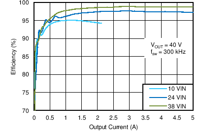 Figure 35. Efficiency of High Voltage Boost Converter Using TPS43060
