SLVSBP4D December 2012 – September 2014 TPS43060 , TPS43061
PRODUCTION DATA.
- 1 Features
- 2 Applications
- 3 Description
- 4 Simplified Schematic
- 5 Revision History
- 6 Pin Configuration and Functions
- 7 Specifications
-
8 Detailed Description
- 8.1 Overview
- 8.2 Functional Block Diagram
- 8.3
Feature Description
- 8.3.1 Switching Frequency
- 8.3.2 Low-Dropout Regulator
- 8.3.3 Input Undervoltage (UV)
- 8.3.4 Enable and Adjustable UVLO
- 8.3.5 Voltage Reference and Setting Output Voltage
- 8.3.6 Minimum On-Time and Pulse Skipping
- 8.3.7 Zero-Cross Detection and Duty Cycle
- 8.3.8 Minimum Off-Time and Maximum Duty Cycle
- 8.3.9 Soft-Start
- 8.3.10 Power Good
- 8.3.11 Overvoltage Protection (OVP)
- 8.3.12 OVP and Current Sense Resistor Selection
- 8.3.13 Gate Drivers
- 8.3.14 Thermal Shutdown
- 8.4 Device Functional Modes
-
9 Application and Implementation
- 9.1 Application Information
- 9.2
Typical Applications
- 9.2.1
Synchronous Boost Converter Typical Application Using TPS43061
- 9.2.1.1 Design Requirements
- 9.2.1.2
Detailed Design Procedure
- 9.2.1.2.1 Selecting the Switching Frequency
- 9.2.1.2.2 Inductor Selection
- 9.2.1.2.3 Selecting the Current Sense Resistor
- 9.2.1.2.4 Output Capacitor Selection
- 9.2.1.2.5 MOSFET Selection - NexFET Power Block
- 9.2.1.2.6 Bootstrap Capacitor Selection
- 9.2.1.2.7 VCC Capacitor
- 9.2.1.2.8 Input Capacitor
- 9.2.1.2.9 Output Voltage and Feedback Resistors Selection
- 9.2.1.2.10 Setting the Soft-Start Time
- 9.2.1.2.11 UVLO Set Point
- 9.2.1.2.12 Power Good Resistor Selection
- 9.2.1.2.13 Control Loop Compensation
- 9.2.1.2.14 DCM, Pulse-Skip Mode, and No-Load Input Current
- 9.2.1.3 Application Curves
- 9.2.2 High-Efficiency 40-V Synchronous Boost Converter Typical Application Using TPS43060
- 9.2.1
Synchronous Boost Converter Typical Application Using TPS43061
- 10Power Supply Recommendations
- 11Layout
- 12Device and Documentation Support
- 13Mechanical, Packaging, and Orderable Information
パッケージ・オプション
メカニカル・データ(パッケージ|ピン)
- RTE|16
サーマルパッド・メカニカル・データ
- RTE|16
発注情報
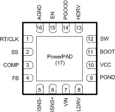
6 Pin Configuration and Functions
WQFN-16 PACKAGE
(TOP VIEW)

Pin Functions
| PIN | DESCRIPTION | |
|---|---|---|
| NAME | NO. | |
| RT/CLK | 1 | Resistor timing and external clock. An external resistor from this pin to the AGND pin programs the switching frequency between 50 kHz and 1 MHz. Driving the pin with an external clock between 300 kHz to 1 MHz synchronizes the switching frequency to the external clock. |
| SS | 2 | Soft-start programming pin. A capacitor between the SS pin and AGND pin sets soft-start time. |
| COMP | 3 | Output of the internal transconductance error amplifier. The feedback loop compensation network is connected from this pin to AGND. |
| FB | 4 | Error amplifier input and feedback pin for voltage regulation. Connect this pin to the center tap of a resistor divider to set the output voltage. |
| ISNS– | 5 | Inductor current sense comparator inverting input pin. This pin is normally connected to the inductor side of the current sense resistor. |
| ISNS+ | 6 | Inductor current sense comparator non-inverting input pin. This pin is normally connected to the VIN side of the current sense resistor. |
| VIN | 7 | The input supply pin to the IC. Connect VIN to a supply voltage between 4.5 and 38 V. It is acceptable for the voltage on the VIN pin to be different from the boost power stage input, ISNS+, and ISNS– pins. |
| LDRV | 8 | Low-side gate driver output. Connect this pin to the gate of the low-side N-channel MOSFET. When VIN bias is removed, an internal 200-kΩ resistor pulls LDRV to PGND. |
| PGND | 9 | Power ground of the IC. Connect this pin to the source of the low-side MOSFET. PGND should be connected to AGND via a single point on the PCB. |
| VCC | 10 | Output of an internal LDO and power supply for internal control circuits and gate drivers. VCC is typically 7.5 V for the TPS43060 and 5.5 V for the TPS43061. Connect a low-ESR ceramic capacitor from this pin to PGND. TI recommends a capacitance range from 0.47 to 10 µF. |
| BOOT | 11 | Bootstrap capacitor node for high-side MOSFET gate driver. Connect the bootstrap capacitor from this pin to the SW pin. For the TPS43060, also connect a bootstrap diode from VCC to BOOT. |
| SW | 12 | Switching node of the boost converter. Connect this pin to the junction of the drain of the low-side MOSFET, the source of high-side synchronous MOSFET, and the inductor. |
| HDRV | 13 | High-side gate driver output. Connect this pin to the gate of the high-side synchronous rectifier MOSFET. When VIN bias is removed, this pin is connected to SW through an internal 200-kΩ resistor. |
| PGOOD | 14 | Power good indicator. This pin is an open-drain output. TI recommends a 10-kΩ pullup resistor between PGOOD and VCC or an external logic supply pin. |
| EN | 15 | Enable pin with internal pullup current source. Floating this pin will enable the IC. Pull below 1.2 V to enter low current standby mode. Pull below 0.4 V to enter shutdown mode. The EN pin can be used to implement adjustable UVLO using two resistors. |
| AGND | 16 | Analog signal ground of the IC. AGND should be connected to PGND at a single point on the PCB. |
| PowerPAD | 17 | The PowerPAD should be connected to AGND. If possible, use thermal vias to connect to an internal ground plane for improved power dissipation. |