SLVSBP4D December 2012 – September 2014 TPS43060 , TPS43061
PRODUCTION DATA.
- 1 Features
- 2 Applications
- 3 Description
- 4 Simplified Schematic
- 5 Revision History
- 6 Pin Configuration and Functions
- 7 Specifications
-
8 Detailed Description
- 8.1 Overview
- 8.2 Functional Block Diagram
- 8.3
Feature Description
- 8.3.1 Switching Frequency
- 8.3.2 Low-Dropout Regulator
- 8.3.3 Input Undervoltage (UV)
- 8.3.4 Enable and Adjustable UVLO
- 8.3.5 Voltage Reference and Setting Output Voltage
- 8.3.6 Minimum On-Time and Pulse Skipping
- 8.3.7 Zero-Cross Detection and Duty Cycle
- 8.3.8 Minimum Off-Time and Maximum Duty Cycle
- 8.3.9 Soft-Start
- 8.3.10 Power Good
- 8.3.11 Overvoltage Protection (OVP)
- 8.3.12 OVP and Current Sense Resistor Selection
- 8.3.13 Gate Drivers
- 8.3.14 Thermal Shutdown
- 8.4 Device Functional Modes
-
9 Application and Implementation
- 9.1 Application Information
- 9.2
Typical Applications
- 9.2.1
Synchronous Boost Converter Typical Application Using TPS43061
- 9.2.1.1 Design Requirements
- 9.2.1.2
Detailed Design Procedure
- 9.2.1.2.1 Selecting the Switching Frequency
- 9.2.1.2.2 Inductor Selection
- 9.2.1.2.3 Selecting the Current Sense Resistor
- 9.2.1.2.4 Output Capacitor Selection
- 9.2.1.2.5 MOSFET Selection - NexFET Power Block
- 9.2.1.2.6 Bootstrap Capacitor Selection
- 9.2.1.2.7 VCC Capacitor
- 9.2.1.2.8 Input Capacitor
- 9.2.1.2.9 Output Voltage and Feedback Resistors Selection
- 9.2.1.2.10 Setting the Soft-Start Time
- 9.2.1.2.11 UVLO Set Point
- 9.2.1.2.12 Power Good Resistor Selection
- 9.2.1.2.13 Control Loop Compensation
- 9.2.1.2.14 DCM, Pulse-Skip Mode, and No-Load Input Current
- 9.2.1.3 Application Curves
- 9.2.2 High-Efficiency 40-V Synchronous Boost Converter Typical Application Using TPS43060
- 9.2.1
Synchronous Boost Converter Typical Application Using TPS43061
- 10Power Supply Recommendations
- 11Layout
- 12Device and Documentation Support
- 13Mechanical, Packaging, and Orderable Information
パッケージ・オプション
メカニカル・データ(パッケージ|ピン)
- RTE|16
サーマルパッド・メカニカル・データ
- RTE|16
発注情報
8 Detailed Description
8.1 Overview
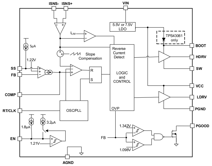
The TPS4306x is a high-performance, wide-input range synchronous boost controller that accepts a 4.5 to 38 V (40-V absolute max) input and support output voltages up to 58 V. The devices have gate drivers for both the low-side N-channel MOSFET and the high-side synchronous rectifier N-channel MOSFET. Voltage regulation is achieved employing constant frequency current mode pulse-duration modulation (PWM) control. The switching frequency is set either by an external timing resistor or by synchronizing to an external clock signal. The switching frequency is programmable from 50 kHz to 1 MHz in the resistor programmed mode or can be synchronized to an external clock between 300 kHz to 1 MHz.
The PWM control circuitry turns on the low-side MOSFET at the beginning of each oscillator clock cycle, as the error amplifier compares the output voltage feedback signal at the FB pin to the internal 1.22-V reference voltage. The low-side MOSFET is turned-off when the inductor current reaches a threshold level set by the error amplifier output. After the low-side MOSFET is turned off, the high-side synchronous MOSFET is turned on until the beginning of the next oscillator clock cycle or until the inductor current reaches the reverse current sense threshold. The input voltage is applied across the inductor and stores the energy as inductor current ramps up during the portion of the switching cycle when the low-side MOSFET is on. Meanwhile, the output capacitor supplies load current. When the low-side MOSFET is turned off by the PWM controller, the inductor transfers stored energy with the synchronous MOSFET to replenish the output capacitor and supply the load current. This operation repeats every switching cycle.
The devices feature internal slope compensation to avoid subharmonic oscillation that is intrinsic to peak current mode control at duty cycles higher than 50%. They also feature adjustable soft-start time, optional lossless inductor DCR current sensing, an output power good indicator, cycle-by-cycle current limit, and overtemperature protection.
8.2 Functional Block Diagram
8.3 Feature Description
8.3.1 Switching Frequency
The switch frequency is set by a resistor (RT) connected to the RT/CLK pin of the TPS4306x. Figure 17 shows the relationship between the timing resistance (RT) and frequency. The resistor value required for a desired frequency can be calculated using Equation 1.

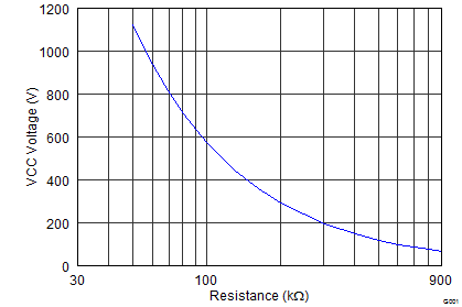 Figure 17. Frequency vs RT Resistance
The device switching frequency can be synchronized to an external clock that is applied to the RT/CLK pin. The external clock should be in the range of 300 kHz to 1 MHz. The required logic levels of the external clock are shown in the specification table. The pulse duration of the external clock should be greater than 20 ns to ensure proper synchronization. A resistor between 57.5 and 1150 kΩ must always be connected from the RT/CLK pin to ground when the converter is synchronized to an external clock. Do not leave this pin open.
8.3.2 Low-Dropout Regulator
The TPS4306x contains a low-dropout regulator that provides bias supply for the controller and the gate driver. The output of the LDO of TPS4306x is regulated to 7.5 and 5.5 V, respectively. When the input voltage is below the VCC regulation level, the VCC output tracks VIN with a small dropout voltage. The output current of the VCC regulator should not exceed 50 mA. The value of the VCC capacitance depends on the total system design and its startup characteristics. The recommended range of values for the VCC capacitor is from 0.47 to 10 µF.
8.3.3 Input Undervoltage (UV)
A UV detection circuit prevents misoperation of the device at input voltages below 3.9 V (typical). When the input voltage is below the VIN UV threshold, the internal PWM control circuitry and gate drivers are turned off. The threshold is set below the minimum operating voltage of 4.5 V to ensure that a transient VIN dip does not cause the device to reset. For input voltages between the UV threshold and 4.5 V, the device attempts to operate, but the electrical specifications are not ensured. The EN pin can be used to achieve adjustable UVLO if the desired start-up threshold is higher than 3.9 V. Details are provided in the following section.
8.3.4 Enable and Adjustable UVLO
The EN pin voltage must be greater than 1.21 V (typical) to enable TPS4306x. The device enters a shutdown mode when the EN voltage is less than 0.4 V. In shutdown mode, the input supply current for the device is less than 5 µA. The EN pin has an internal 1.8-μA pullup current source that provides the default enabled condition when the EN pin floats. When the EN pin voltage is higher than the shutdown threshold but less than 1.21 V, the devices are in standby mode.
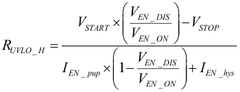
Adjustable input UVLO can be accomplished using the EN pin. As shown in Figure 18, a resistor divider from the VIN pin to AGND sets the UVLO level. When EN pin voltage crosses the 1.21 V (typical) threshold voltage, an additional 3.2-μA hysteresis current is sourced out of the EN pin. When the EN pin voltage falls below 1.14 V (typical), the hysteresis current is removed. The addition of hysteresis current at the EN threshold facilitates adjustable input voltage hysteresis. RUVLO_H and RUVLO_L are calculated using Equation 2 and Equation 3, respectively.
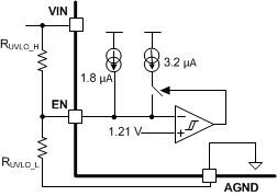 Figure 18. Adjustable UVLO Using EN Pin

where
- VSTART is the desired turn-on voltage at the VIN pin.
- VSTOP is the desired turn-off voltage at the VIN pin.
- VEN_ON is the EN pin voltage threshold to enable the device, 1.21 V (typical).
- VEN_DIS is the EN pin voltage threshold to disable the device, 1.14 V (typical).
- IEN_hys is the hysteresis current inside the device, 3.2 μA (typical).
- IEN_pup is the internal pullup current at EN pin, 1.8 μA (typical).
8.3.5 Voltage Reference and Setting Output Voltage
An internal voltage reference provides a precise 1.22-V voltage reference at the error amplifier non-inverting input. To set the output voltage, select the FB pin resistor RSH and RSL according to Equation 4.

8.3.6 Minimum On-Time and Pulse Skipping
The TPS4306x also features a minimum on-time of 100 ns for the low-side gate driver. This minimum on-time determines the minimum duty cycle of the PWM for any set switching frequency. When the voltage regulation loop requires a minimum on-time pulse duration less than 100 ns, the controller enters pulse-skipping mode. In this mode, the devices hold the power switch off for multiple switching cycles to prevent the output voltage from rising above the desired regulated voltage. This operation typically occurs in light load conditions when the DC-DC converter operates in discontinuous conduction mode (DCM). Pulse skipping increases the output ripple as shown in Figure 27.
8.3.7 Zero-Cross Detection and Duty Cycle
The TPS4306x features zero-cross detection, which turns off the high-side driver when the sensed current falls below the reverse current sense threshold (3.8 mV typical), then the converter runs in DCM. The duty cycle is dependent on the mode in which the converter is operating. The duty cycle in DCM varies widely with changes of the load. In continuous conduction mode (CCM), where the inductor maintains a minimum dc current, the duty cycle is related primarily to the input and output voltages as computed in Equation 5.

When the converter operates in DCM, the duty cycle is a function of the load, input and output voltages, inductance, and switching frequency in Equation 6.

Equation 5 and Equation 6 provide an estimation of the duty cycle. A more accurate duty cycle can be calculated by including the voltage drops of the external MOSFETs, sense resistor, and DCR of the inductor.
8.3.8 Minimum Off-Time and Maximum Duty Cycle
The low-side driver LDRV of TPS4306x has a minimum off-time of 250 ns or 5% of the switching cycle period, whichever is longer. Figure 19 shows maximum duty cycle versus switching frequency. The maximum duty cycle limits the maximum achievable step-up ratio in a boost converter. When the converter operates in CCM, the step-up ratio of the boost converter can be calculated using Equation 7.

For instance, if the maximum duty cycle is 90%, the achievable maximum output voltage to input voltage ratio is limited to:

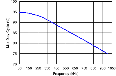 Figure 19. Maximum Duty Cycle vs Frequency
8.3.9 Soft-Start
The TPS4306x has a built-in soft-start circuit, which significantly reduces the start-up current spike and output voltage overshoot. When the IC is enabled, an internal bias current source (5 µA typical) charges the capacitor (CSS) on the SS pin. When the SS pin voltage is less than the internal 1.22-V reference, the device regulates the FB pin voltage to the SS pin voltage rather than the internal 1.22-V reference voltage. When the SS pin voltage exceeds the reference voltage, the device regulates the FB pin voltage to 1.22 V. The soft-start time of the output voltage can be calculated using Equation 9.

8.3.10 Power Good
The TPS4306x PGOOD pin indicates when the output voltage is within predetermined limits of the desired regulated output voltage by monitoring the FB pin voltage. The PGOOD pin is driven by the open-drain signal of an internal MOSFET. When the output voltage of the power converter is not within ±10% of the output voltage set point, the PGOOD MOSFET turns on and pulls the PGOOD pin low. Otherwise, the PGOOD MOSFET stays off and the PGOOD pin can be pulled up by an external resistor to a voltage supply up to 8 V.
The PGOOD signal is also pulled low if the EN voltage or VIN voltage is below their respective voltage thresholds.
8.3.11 Overvoltage Protection (OVP)
The TPS4306x integrates an OVP circuit that turns off the low-side MOSFET when the output voltage reaches the OVP threshold, which is internally fixed to 107% of the output voltage set point. The low-side MOSFET resumes normal PWM control when the output voltage drops below 105% of the output voltage set point. The OVP circuit protects the power MOSFETs and minimizes the output voltage overshoot during transients or fault conditions.
8.3.12 OVP and Current Sense Resistor Selection
The TPS4306x provides cycle-by-cycle current limit protection that turns off the low-side MOSFET when the inductor current reaches the current limit threshold. The cycle-by-cycle current limit circuitry is reset at the beginning of the next switching cycle. During an overcurrent event, the output voltage begins to droop as a function of the load on the output.
A slope compensation ramp is added to the current sense ramp to prevent subharmonic oscillations at high duty cycle. The slope compensation reduces the overcurrent limit threshold (maximum current sense threshold) with increasing duty cycle as detailed in Figure 20.
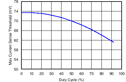 Figure 20. Overcurrent Limit Threshold With Respect to Duty Cycle
The maximum current sense threshold VCSmax sets the maximum peak inductor current, which is the sum of maximum average inductor (input) current, Iave_max, and half the peak-to-peak inductor ripple, ΔIL. Choose the sense resistor value based on the desired maximum input current and the ripple current, which can be calculated using Equation 10.

8.3.13 Gate Drivers
The TPS4306x contains powerful high-side and low-side gate drivers supplied by the VCC bias regulator. The nominal VCC voltage of the TPS43060 and TPS43061 is 7.5 V and 5.5 V, respectively. The TPS43061 gate drivers operate from a 5.5-V VCC supply, with drive strength optimized for low Qg NexFETs. It also features an integrated bootstrap diode for the high-side gate driver to reduce the external part count. The TPS43060 gate drivers operate from a 7.5-V VCC supply, which is suitable to drive a wide range of standard MOSFETs. The TPS43060 requires an external bootstrap diode from VCC to BOOT to charge the bootstrap capacitor. It also requires a 2-Ω resistor connected in series with the VCC pin to limit the peak current drawn through the internal circuitry when the external bootstrap diode is conducting. See the Electrical Characteristics for typical rise and fall times and the output resistance of the gate drivers.
The LDRV and HDRV outputs are controlled with an adaptive dead-time control that ensures both the outputs are never high at the same time. This minimizes any cross conduction and protects the power converter. The typical dead-time from LDRV fall to HDRV rise is 65 ns.
The Qg versus VGS and the VGS versus RDS(on) curves for a given MOSFET should be used to determine which gate drive voltage is appropriate. For example, the CSD86330Q3D synchronous power block has sufficient gate drive voltage for low RDS(on) with the 5.5-V gate drive of the TPS43061. However, the CSD18537NQ5A MOSFET has better RDS(on) performance with the 7.5-V gate drive of the TPS43060.
The designer needs to make important considerations if the stronger gate drivers of the TPS43060 are used with low Qg and low-voltage threshold MOSFETs. The stronger gate driver causes the low-side MOSFET to turn on very quickly resulting in large voltage undershoot below PGND at the SW node. The BOOT capacitor then temporarily has a voltage across it exceeding the 8-V absolute maximum ratings. The external BOOT Schottky diode with fast-switching speeds allows the BOOT capacitor to receive some charge during this short time period. At light loads when the high-side MOSFET is not switching, there is no load on the BOOT capacitor. The BOOT capacitor can then charge to a voltage exceeding the absolute maximum ratings. To limit the voltage across the BOOT-SW pins, the RC time constant for charging the BOOT capacitor should be increased to avoid charging while the SW node is below ground and/or the SW voltage undershoot should be reduced. Do this by following these recommendations:
- Resistor in series with the external Schottky diode to increase RC time constant for charging the BOOT capacitor
- Resistor in series with the LDRV signal to slow down the low-side MOSFET switching speed and reduce SW ringing
- RC snubber across the high-side MOSFET to reduce SW ringing
- Proper layout techniques as recommended in Layout to reduce SW ringing
Figure 21 shows these components. A typical value for either series resistor is 4.7 Ω.
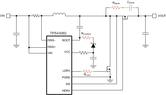 Figure 21. External Components for Limiting the BOOT-SW Voltage
8.4 Device Functional Modes
8.4.1 Typical Operation (VIN < VOUT)
The TPS4306x is designed to operate with a minimum input voltage of 4.5 V. It will turn on when the VIN voltage exceeds the typical 4.1-V UVLO threshold and the EN voltage exceeds the typical 1.21-V enable voltage threshold. If EN is left floating, an internal current source pulls the voltage above the EN threshold. In a boost topology, the input is passed to the output through the inductor and high-side FET body diode. As a result, while the TPS4306x is disabled, the output voltage will track the input voltage. When both thresholds are exceeded, the VCC LDO output comes into regulation. Switching is enabled and the SS current source begins charging the external soft-start capacitor for a controlled soft-start of the output voltage with a time period determined by the value of the external SS capacitor. If either pin's voltage drops below its respective threshold, the TPS4306x is shutdown.
8.4.2 Pass Through (VIN > VOUT)
If there is an operation condition where the input voltage exceeds the output voltage set by the external FB resistor divider, the TPS4306x stops switching. The input voltage is directly connected to the output voltage through the inductor and body diode of the external high-side MOSFET. The output voltage then follows the input voltage with a voltage drop determined mainly by the forward voltage of the high-side MOSFET body diode. If there is an output load while in this mode, pay attention to power dissipation in the high-side MOSFET body diode. The TPS4306x begins switching again after the input voltage drops below the output voltage set by the external FB resistor divider.
8.4.3 Split-Rail Operation
The TPS4306x can also operate in a split-rail topology where a separate voltage is provided to bias the VIN pin of the IC to 4.5 V or greater. The power for the boost power stage can then be powered from a separate input lower than the 4.5-V minimum VIN voltage. When operating in this mode, the boost power stage voltage must be greater than 2.5 V to bias the ISNS pins or the current limit accuracy may degrade. If used in split rail, the TPS4306x is enabled and disabled in the same VIN and EN conditions as described in Typical Operation (VIN < VOUT).