JAJSF84B December 2008 – May 2018 TPS650250
PRODUCTION DATA.
- 1 特長
- 2 アプリケーション
- 3 概要
- 4 改訂履歴
- 5 Pin Configuration and Functions
-
6 Specifications
- 6.1 Absolute Maximum Ratings
- 6.2 ESD Ratings
- 6.3 Recommended Operating Conditions
- 6.4 Thermal Information
- 6.5 Dissipation Ratings
- 6.6 Electrical Characteristics
- 6.7 Electrical Characteristics VDCDC1
- 6.8 Electrical Characteristics VDCDC2
- 6.9 Electrical Characteristics VDCDC3
- 6.10 Typical Characteristics
- 7 Detailed Description
- 8 Application and Implementation
- 9 Power Supply Recommendations
- 10Layout
- 11デバイスおよびドキュメントのサポート
- 12メカニカル、パッケージ、および注文情報
パッケージ・オプション
メカニカル・データ(パッケージ|ピン)
- RHB|32
サーマルパッド・メカニカル・データ
- RHB|32
発注情報
8.2.3.4 Output Voltage Selection
The DEFDCDC1, DEFDCDC2, and DEFDCDC3 pins are used to set the output voltage for each step-down converter. See Table 6 for the default voltages if the pins are pulled to GND or to Vcc.
Table 6. Voltage Options
| PIN | LEVEL | DEFAULT OUTPUT VOLTAGE | |
|---|---|---|---|
| DEFDCDC1 | VCC | 3.3 V | |
| GND | 2.80 V | ||
| DEFDCDC2 | VCC | 2.5 V | |
| GND | 1.8 V | ||
| DEFDCDC3 | external voltage divider | 0.6 V to VinDCDC3 | |
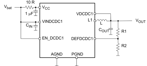
If a different voltage is needed, an external resistor divider can be added to the DEFDCDC1 or DEFDCDC2 pin as shown in Figure 8:
 Figure 8. External Resistor Divider Added
 When a resistor divider is connected to DEFDCDC1 or DEFDCDC2, the output voltage can be set from 0.6 V up to the input voltage Vbat. The total resistance (R1+R2) of the voltage divider should be kept in the 1 MΩ range in order to maintain a high efficiency at light load. VDEFDCDCx = 0.6V
