SLUSAQ9B December 2011 – December 2015 UC1875-SP
PRODUCTION DATA.
- 1 Features
- 2 Applications
- 3 Description
- 4 Revision History
- 5 Description (continued)
- 6 Pin Configuration and Functions
- 7 Specifications
- 8 Detailed Description
-
9 Application and Implementation
- 9.1 Application Information
- 9.2
Typical Application
- 9.2.1 Design Requirements
- 9.2.2
Detailed Design Procedure
- 9.2.2.1 Phase-Shifted Fundamentals
- 9.2.2.2 Circuit Schematic and Description
- 9.2.2.3 Initial Conditions (Time: t = t(0))
- 9.2.2.4 Right Leg Resonant Transition Interval (Time: t(0) < t < t(1))
- 9.2.2.5 Clamped Freewheeling Interval (Time: t(1) < t < t(2))
- 9.2.2.6 Left Leg Transition Interval (Time: t(2) < t < t(3))
- 9.2.2.7 Power Transfer Interval (Time: t(3) < t < t(4))
- 9.2.2.8 Switch Turn Off (Time: t(4))
- 9.2.2.9 Resonant Tank Considerations
- 9.2.2.10 Resonant Circuit Limitations
- 9.2.2.11 Stored Inductive Energy
- 9.2.2.12 Resonant Circuit Summary
- 9.2.2.13 Stored Energy Requirements
- 9.2.2.14 Minimum Primary Current
- 9.2.3 Application Curve
- 10Power Supply Recommendations
- 11Layout
- 12Device and Documentation Support
- 13Mechanical, Packaging, and Orderable Information
パッケージ・オプション
メカニカル・データ(パッケージ|ピン)
サーマルパッド・メカニカル・データ
発注情報
9 Application and Implementation
NOTE
Information in the following applications sections is not part of the TI component specification, and TI does not warrant its accuracy or completeness. TI’s customers are responsible for determining suitability of components for their purposes. Customers should validate and test their design implementation to confirm system functionality.
9.1 Application Information
9.1.1 Undervoltage Lockout Section
When power is applied to the circuit and VIN is below the upper UVLO threshold, IIN will be below 600 µA, the reference generator will be off, the fault latch is reset, the soft-start pin is discharged, and the outputs are actively held low. When VIN exceeds the upper UVLO threshold, the reference generator turns on. All else remains in the shut-down mode until the output of the reference, VREF, exceeds 4.75 V.
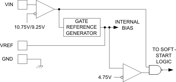 Figure 3. Undervoltage Circuit
The high frequency oscillator may be either free-running or externally synchronized. For free-running operation, the frequency is set via an external resistor and capacitor to ground from the FREQSET pin.
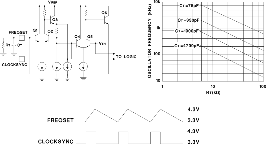 Figure 4. Simplified Oscillator Schematic
9.1.2 Synchronizing the Oscillator
The CLOCKSYNC pin of the oscillator may be used to synchronize multiple UC1875-SP device by connecting the CLOCKSYNC of each UC1875-SP to the others:
 Figure 5. Synchronizing Multiple UC1875-SP
ALL ICs will sync to the chip with the fastest local oscillator.
R1 and RN may be needed to keep sync pulse narrow due to capacitance on line.
R1 and RN may also be needed to properly terminate R(SYNC) line.
9.1.3 Syncing to External TTL/CMOS
 Figure 6. Synchronizing UC1875-SP
ICs will sync to the fastest chip or TTL clock if it is higher frequency.
R1 and RN may be needed to keep sync pulse narrow due to capacitance on line.
R1 and RN may also be needed to properly terminate R(SYNC) line.
Although the UC1875-SP has a local oscillator frequency, the device will synchronize to the fastest oscillator driving the CLOCKSYNC pin. This arrangement allows the synchronizing connection between ICs to be broken without any local loss of functionality.
Synchronizing the device to an external clock signal may be accomplished with a minimum of external circuitry, as shown in Figure 6.
Capacitive loading on the CLOCKSYNC pin will increase the clock pulse width, and may adversely effect system performance. Therefore, a resistor to ground from the CLOCKSYNC pin is optional, but may be required to offset capacitive loading on this pin. These resistors are shown in the oscillator schematics as R1, RN.
9.1.4 Delay Blocks and Output Stages
In each of the output stages, transistors Q3 through Q6 form a high-speed totem-pole driver which will source or sink more than one amp peak with a total delay of approximately 30 nanoseconds. To ensure a low output level prior to turn-on, transistors Q7 through Q9 form a self-biased driver to hold Q6 on prior to the supply reaching its turn-on threshold. This circuit is operable when the chip supply is zero. Q6 is also turned on and held low with a signal from the fault logic portion of the chip.
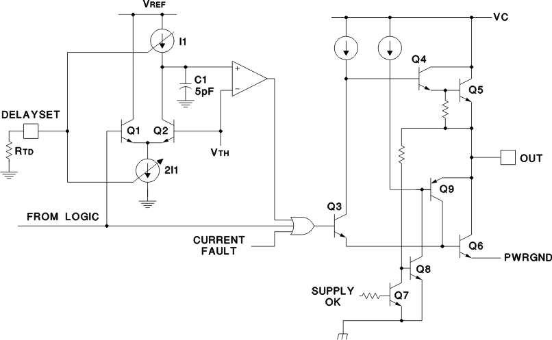 Figure 7. UC1875-SP Output Stage
The delay providing the dead-time is accomplished with C1 which must discharge to VTH before the output can go high. The time is defined by the current sources, I1, which is programmed by an external resistor, RTD. The voltage on the Delay Set pins is internally regulated to 2.5 V and the range of dead time control is from 50 to 200 nanoseconds.
NOTE
There is no way to disable the delay circuitry, and the delay time must be programmed.
9.1.5 Output Switch Orientation
The four outputs of the UC1875-SP interfaces to the full bridge converter switches as shown in Figure 8
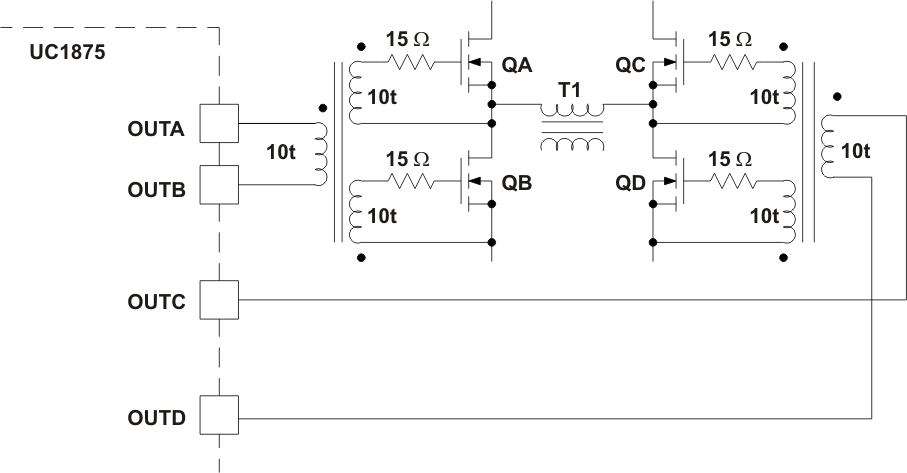 Figure 8. 3 Winding Bifilar, AWG 30 Kynar Insulation
9.1.6 Fault/Soft Start
The fault control circuitry provides two forms of power shutdown:
- Complete turn-off of all four output power stages.
- Clamping the phase shift command to zero.
Complete turn-off is ordered for an over-current fault or a low supply voltage. When the SOFTSTART pin reaches its low threshold, switching is allowed to proceed while the phase-shift is advanced from zero to its nominal value with the time constant of the SOFT-START capacitor.
The fault logic insures that a continuous fault will institute a low frequency “hiccup” retry cycle by forcing the SOFT-START capacitor to charge through its full cycle between each restart attempt.
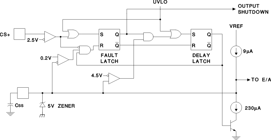 Figure 9. Fault and Restart
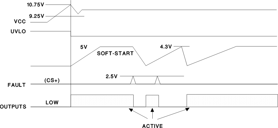 Figure 10. Fault Restart Waveform
9.1.7 Slope/Ramp Pins
The ramp generator may be configured for the following control methods:
- Voltage Mode
- Voltage Feedforward
- Current Mode
- Current Mode with Slope Compensation
Figure 11 shows a voltage-mode configuration. With R(SLOPE) tied to a stable voltage source, the waveform on C(RAMP) will be a constant-slope ramp, providing conventional voltage-mode control. If R(SLOPE) is connected to the power supply input voltage, a variable-slope ramp will provide voltage feedforward.
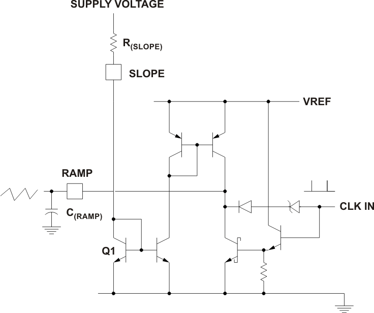 Figure 11. Voltage Mode Operation
- Simple voltage mode operation achieved by placing R(SLOPE) between VIN and SLOPE
- Voltage Feedforward achieved by placing R(SLOPE) between supply voltage and SLOPE pin of UC1875-SP.
RAMP:

For current-mode control the ramp generator may be disabled by grounding the slope pin and using the ramp pin as a direct current sense input to the PWM comparator.
9.2 Typical Application
A typical application for the phase-shifted bridge is to convert high-input voltage to low-output voltage while also providing system isolation.
Using this phase-shifted technique, two of the switches in series with the transformer can be ON, yet the applied voltage to the transformer is zero. These are not diagonal switches of the full-bridge converter, but either the two upper or two lower switches. In this mode, the transformer primary is essentially short circuited and clamped to the respective input rail. Primary current is maintained at its previous state because there is no voltage available for reset to take place. This deadband fills the void between the resonant transitions and power-transfer portion of the conversion cycle. Switches can be held in this state for a certain period of time which corresponds to the required off time for that particular switching cycle.
When the correct one of these switches is later turned off, the primary current flows into the switch output capacitance (Coss) causing the switch drain voltage to resonate to the opposite input rail. This aligns the opposite switch of the particular bridge leg with zero voltage across it, enabling zero-voltage switching when it is turned ON.
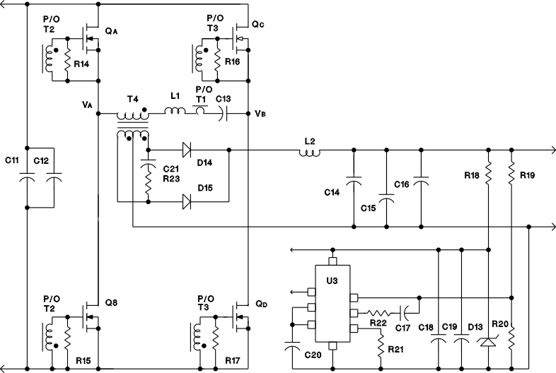 Figure 12. Phase-Shifted PWM Converter Control and Output Circuit Schematic
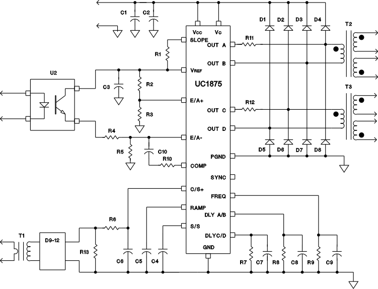 Figure 13. Phase Shifted PWM Converter Control and Drive Circuit Schematic
9.2.1 Design Requirements
Table 2 lists the requirements for this application. Further requirements can be found in Phase Shifted, Zero Voltage Transition Design Considerations and the UC3875 PWM Controller (SLUA107).
Table 2. Design Parameters
| PARAMETER | VALUE |
|---|---|
| Vin | 48 V |
| Vout | 5 V at 40 A |
9.2.2 Detailed Design Procedure
9.2.2.1 Phase-Shifted Fundamentals
Switches within the phase-shifted full bridge converter will be utilized differently than those of its non-resonant counterpart. Instrumental to this technique is the use of the parasitic elements of the MOSFET switch’s construction. The internal body diode and output capacitance (Coss) of each device (in conjunction with the primary current) become the principal components used to accomplish and commutate the resonant transitions.
9.2.2.2 Circuit Schematic and Description
A more detailed operation of the phase-shifted converter operation follows a description of the circuit elements. The circuit schematic of this technique is shown in Figure 14, including voltage and current designations.
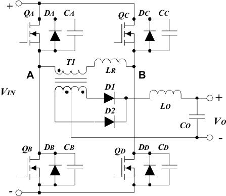 Figure 14. Phase-Shifted PWM Switch Orientation
The basic circuit is comprised of four switches labeled QA through QD and is divided up into two “legs”, the right and left hand legs. Each switch is shown shunted by its body diode (DA through DD) and parasitic output capacitance, (CA through CD). These have been identified separately to clarify the exact elements and current paths during the conversion interval.
A detailed model of the transformer primary section is presented which separately indicates the leakage and magnetizing inductances and currents of the primary. The reflected secondary contributors to primary current are also shown for completeness, and divided into two components. The DC primary current (IP) is the secondary DC output current divided by the transformer turns ratio (N). The secondary AC current should also be accounted for by multiplying the output inductance by the turns ratio squared (N2), or dividing the secondary AC ripple current ISEC(ac) by the turns ratio (N) as shown in Figure 15.
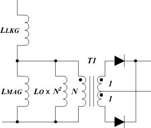 Figure 15. Primary Magnetic Components
9.2.2.3 Initial Conditions (Time: t = t(0))
The description of the Phase Shifted operation will begin with the conclusion of one power transfer cycle. This occurs when the transformer had been delivering power to the load and two of diagonal switches of the converter were conducting. The initial current flowing in the primary can be designated as IP(t(0)).
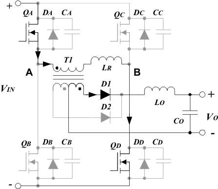 Figure 16. Initial Conditions
9.2.2.4 Right Leg Resonant Transition Interval (Time: t(0) < t < t(1))
The primary current flowing at time t(0) is equal to IP(t(0)) and was being conducted through the diagonal set of transistors QA in the upper left hand corner of the bridge and transistor QD in the lower right. Instantly, at time t(0) switch QD is turned off by the control circuitry which begins the resonant transition of the right hand leg of the converter.
The primary current flowing is maintained nearly constant at IP(t(0)) by the resonant inductance of the primary circuit, often referred to as the transformers leakage inductance. Since an external series inductance can be added to alter the effective leakage inductance value, this presentation will refer to the lumped sum of these inductors as the resonant inductance, LR. In a practical application it may be difficult to accurately control the transformers leakage inductance within an acceptable ZVS range, necessitating an external “shim” inductor to control the accuracy. It’s also possible that the transformer leakage inductance can be too low to provide the desired transition times for the application so an external inductor can be introduced to modify the resonant inductance.
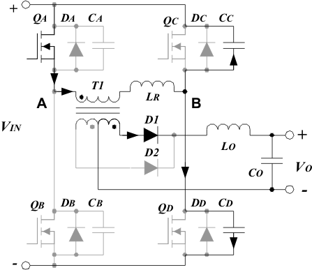 Figure 17. Right Leg Transition
With switch QD turned off, the primary current continues to flow using the switch output capacitance, CD to provide the path. This charges the switch capacitance of QD from essentially zero volts to the upper voltage rail, Vin+. Simultaneously, the transformer capacitance (Cxfmr) and the output capacitance of switch QC is discharged as its source voltage rises from the lower to the upper rail voltage. This resonant transition positions switch QC with no drain to source voltage prior to turn-on and facilitates lossless, zero voltage switching.
The primary current causing this right leg transition can be approximated by the full load primary current of IP(t(0)). The small change due to the barely resonant circuit contribution is assumed to be negligible in comparison to the magnitude of the full load current.
During this right leg transition the voltage across the transformers primary has decreased from VIN to zero. At some point in the transition the primary voltage drops below the reflected secondary voltage, VO x N. When this occurs the primary is no longer supplying full power to the secondary and the output inductor voltage changes polarity. Simultaneously, energy stored in the output choke begins supplementing the decaying primary power until the primary contribution finally reaches zero.
Once the right leg transition has been completed there is no voltage across the transformer primary. Likewise, there is no voltage across the transformers secondary winding and no power transferred, assuming ideal conditions. Note that the resonant transition not only defines the rate of change in primary and secondary voltages dV/dt, but also the rate of change in current in the output filter network, dI/dt.
9.2.2.5 Clamped Freewheeling Interval (Time: t(1) < t < t(2))
Once the right leg transition is complete the primary current free wheels through transistor QA and the body diode of switch QC. The current would remain constant until the next transition occurs assuming that the components were ideal. Switch QC can be turned on at this time which shunts the body diode with the FET Rds(on) switch impedance thus lowering conduction losses. Although current is flowing opposite to the normal convention (source to drain) the channel of QC will conduct and divide the current between the switch and body diode.
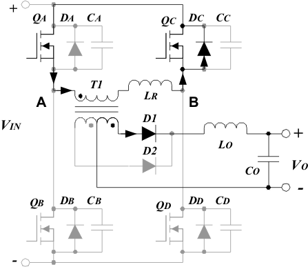 Figure 18. Clamped Free Wheeling Interval
9.2.2.6 Left Leg Transition Interval (Time: t(2) < t < t(3))
At time t(2) a residual current was flowing in the primary of the transformer which is slightly less than IP(t(0)) due to losses. Switch QC has been previously turned ON and switch QA will now be turned OFF. The primary current will continue to flow but the path has changed to the output capacitance (CA) of switch QA instead of its channel. The direction of current flowing causes the drain to source voltage of switch QA to increase and lowers its source from the upper to lower rail voltage. Just the opposite conditions have occurred to switch QB which previously had the full input across its terminals. The resonant transition now aligns switch QB with zero voltage across it, enabling lossless switching to occur.
Primary current continues to flow and is clamped by the body diode of switch QB, which is still OFF. This clamping into a short circuit is a necessary condition for fixed frequency, zero voltage switching. Once switch QB is turned ON, the transformer primary is placed across the input supply rails since switch QC is already ON and will begin to transfer power. Although zero voltage switching has already been established, turning ON switch QB the instant it reaches zero voltage will cause variable frequency operation.
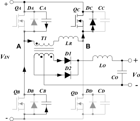 Figure 19. Left Leg Transition
Note that this left leg transition will require more time to complete than the right leg transition. Conduction losses in the primary switches, transformer winding and interconnections result in a net DC voltage drop due to the flowing primary current. Energy stored in the series resonant inductor and magnetizing inductance is no longer ideally clamped to zero voltage. This loss, in addition to the losses incurred during the previous transition, reduce the primary current below its initial IP(t(0)) value, thus causing a longer left leg transition time than the right leg.
Unlike conventional power conversion, one transistor in the diagonal pair of the phase shifted full bridge converter is ON just before power is transferred which simplifies the gate drive. An additional benefit is realized by designating these commutating switches as the high side switches of the converter, usually far more difficult to drive than their lower side counterparts.
9.2.2.7 Power Transfer Interval (Time: t(3) < t < t(4))
This interval of the phase shifted cycle is basically identical to that of conventional square wave power conversion. Two diagonal switches are ON which applies the full input voltage across the transformer primary. Current rises at a rate determined by VIN and the series primary inductance, however starts at a negative value as opposed to zero. The current will increase to a DC level equal to the output current divided by the turns ratio, IO/N. The two time variant contributors to primary current are the magnetizing current (IMAG) and the output inductor magnetizing contribution reflected to the primary, LO x N2. The exact switch ON time is a function of VIN, VO and N the transformer turns ratio, just as with conventional converters.
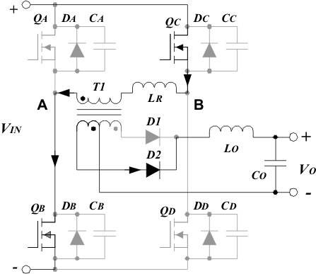 Figure 20. Power Transfer Interval
9.2.2.8 Switch Turn Off (Time: t(4))
One switching cycle is concluded at time t(4) when QC the upper right hand corner switch is turned OFF. Current stops flowing in QC’s semiconductor channel but continues through the parasitic output capacitance, CC. This increases the drain-to-source voltage from essentially zero to the full input supply voltage, VIN. The output capacitance of the lower switch in the right hand leg (QD) is simultaneously discharged via the primary current. Transistor QD is then optimally positioned for zero voltage switching with no drain-to-source voltage. The current during this interval is assumed to be constant, simplifying the analysis. In actuality, it is slightly resonant as mentioned in the left leg transition, but the amplitude is negligible in comparison to the full load current. The power conversion interval is concluded at this point and an identical analysis occurs as for the opposite diagonal switch set which has thoroughly been described for the switch set QA and QD.
9.2.2.9 Resonant Tank Considerations
The design of the resonant tank begins with the selection of an acceptable switching frequency; one selected to meet the required power density. Second, the maximum transition time must also be established based on achievable duty cycles under all operating conditions. Experience may provide the best insight for acceptable results.
NOTE
The maximum transition time will occur during the converters left leg transition operating at the minimum output load current.
9.2.2.10 Resonant Circuit Limitations
Two conditions must be met by the resonant circuit at light load, and both relate to the energy stored in the resonant inductor. One, there must be enough inductive energy stored to drive the resonant capacitors to the opposite supply rail. Two, this transition must be accomplished within the allocated transition time. Lossy, non-zero voltage switching will result if either, or both are violated. The first condition will always be met when the latter is used as the resonant circuit limitation.
Designers can argue that some switching loss may be of little consequence in a practical application at very light loads - especially considering that there is a significant benefit at heavy loads. While this may be a pragmatic approach in many applications, and a valid concern, this presentation will continue using the fully lossless mode as the ultimate design goal.
The stored inductive energy requirement and specified maximum transition time have also defined the resonant frequency (ωR) of the tank circuit. Elements of this tank are the resonant inductor (LR) and capacitor (CR), formed by the two switch output capacitors, also in parallel with the transformer primary capacitance Cxfmr. The maximum transition time cannot exceed one-fourth of the self resonant period, (four times the self resonant frequency) to satisfy the zero voltage switching condition.
The resonant tank frequency, ωR:


Coss, the specified MOSFET switch output capacitance will be multiplied by a 4/3 factor to accommodate the increase caused by high voltage operation. During each transition, two switch capacitances are driven in parallel, doubling the total capacitance to 8/3 x Coss. Transformer capacitance (Cxfmr) must also be added as it is NOT negligible in many high frequency applications.
The resonant capacitance, CR:

The capacitive energy required to complete the transition, W(CR) is:

This energy can also be expressed as:

9.2.2.11 Stored Inductive Energy
The energy stored in the resonant inductance must be greater than the energy required to charge and discharge the FET output and transformer capacitances of the leg in transition within the maximum transition time.
Inside the transformer, all of the energy is stored in the leakage inductance since the secondary current has clamped the transformers primary voltage to essentially zero. This causes high circulating primary current (as shown in figure 8) in the physical winding but has no effect on the stored energy used to perform the ZVS transition. More detail about the tradeoffs and design optimization is presented in the Design Procedure.
The energy stored in the resonant inductor, LR:

9.2.2.12 Resonant Circuit Summary
There are several ways to arrive at the solutions for the resonant inductor value and minimum primary current required for any application. Each of these is based upon the following fundamental relationships. The resonant tank frequency must be at least four times higher than the transition time to fully resonate within the maximum transition time tMAX at light load.


Where:


Reorganizing and combining these relationships;


The resonant radian frequency (ωR) is related to the resonant components by the equation:

Both sides of this can be squared to simplify the calculations and reorganized to solve for the exact resonant inductor value.

Previously outlined relationships for ωR and CR can be introduced to result in the following specific equation.

NOTE
This figure indicates the exact resonant inductor value required to satisfy only the task of resonant transitions. This resonant inductor is in series with the transformer primary hence also defines the maximum primary current slew rate, dI/dt as a function of input voltage.

If the resonant inductor value is too large it may take too long to reach the necessary load current within the conversion cycle. The calculated inductor value satisfies the light load condition, however full load operation must also be evaluated. Details of possible solutions to this are highlighted in the Practical Applications section of this paper.
9.2.2.13 Stored Energy Requirements
As detailed, the energy stored in the resonant inductor must be greater than the capacitive energy required for the transition to occur within the allocated transition time. The governing equations are summarized below.


Since CR and VIN are known or can be estimated for a given application, this term becomes a constant and LR has been quantified.
9.2.2.14 Minimum Primary Current
The minimum primary current required for the phase shifted application can now be determined by reorganizing the previous equation.

This value can be supported by the calculating the average current required to slew the resonant capacitor to the full rail voltage. Although this figure will be lower that IP(MIN) it can be used as a confirmation of the mathematics.

Obtaining the necessary amount of primary current can be done in several ways. The most direct approach is to simply limit the minimum load current to the appropriate level. One alternative, however, is to design the transformer magnetizing inductance accordingly. Also assisting the magnetizing current is the reflected secondary inductor current contribution which is modeled in parallel. Any duty cycle variations modifying the peak charging current must also be taken into account.
Generally the magnetizing current alone is insufficient in many off-line high frequency converters. The transformer is usually core loss limited which means numerous primary turns and a high magnetizing inductance. Shunting the transformer primary with an external inductor to develop the right amount of primary current is one possibility. Incorporating the output filter inductor magnetizing current to assist resonance on the primary side is also an alternative.
9.2.3 Application Curve
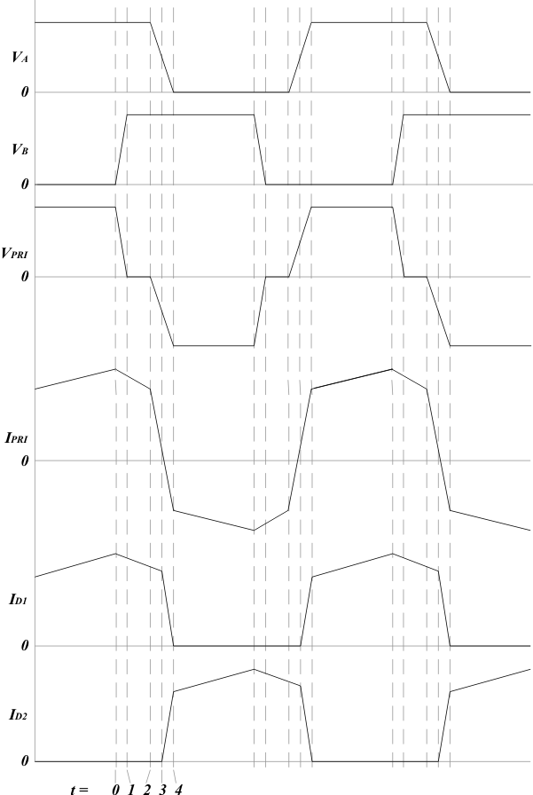 Figure 21. Operational Waveforms