SLUSAQ9B December 2011 – December 2015 UC1875-SP
PRODUCTION DATA.
- 1 Features
- 2 Applications
- 3 Description
- 4 Revision History
- 5 Description (continued)
- 6 Pin Configuration and Functions
- 7 Specifications
- 8 Detailed Description
-
9 Application and Implementation
- 9.1 Application Information
- 9.2
Typical Application
- 9.2.1 Design Requirements
- 9.2.2
Detailed Design Procedure
- 9.2.2.1 Phase-Shifted Fundamentals
- 9.2.2.2 Circuit Schematic and Description
- 9.2.2.3 Initial Conditions (Time: t = t(0))
- 9.2.2.4 Right Leg Resonant Transition Interval (Time: t(0) < t < t(1))
- 9.2.2.5 Clamped Freewheeling Interval (Time: t(1) < t < t(2))
- 9.2.2.6 Left Leg Transition Interval (Time: t(2) < t < t(3))
- 9.2.2.7 Power Transfer Interval (Time: t(3) < t < t(4))
- 9.2.2.8 Switch Turn Off (Time: t(4))
- 9.2.2.9 Resonant Tank Considerations
- 9.2.2.10 Resonant Circuit Limitations
- 9.2.2.11 Stored Inductive Energy
- 9.2.2.12 Resonant Circuit Summary
- 9.2.2.13 Stored Energy Requirements
- 9.2.2.14 Minimum Primary Current
- 9.2.3 Application Curve
- 10Power Supply Recommendations
- 11Layout
- 12Device and Documentation Support
- 13Mechanical, Packaging, and Orderable Information
パッケージ・オプション
メカニカル・データ(パッケージ|ピン)
サーマルパッド・メカニカル・データ
発注情報
11 Layout
11.1 Layout Guidelines
Connect Vin pin to bias supply from 10.75 V to 18 V range. Place high quality, low ESR and ESL, at least 1-μF ceramic bypass capacitor CVDD from this pin to GND. It is recommended to use 10-Ω resistor in series to VDD pin to form RC filter with CVDD capacitor.
11.1.1 Ground (GND)
All signals are referenced to this node. It is recommended to have a separate quite analog plane connected in one place to the power plane. The analog plane combines the components related to the pins VREF, E/A out, EA+, EA-, CS+, SoftStart, DELAYSET A-B, DELAYSET C-D, VC, RAMP, SLOPE, CLOCKSYNC, FREQSET, GND and VIN. The power plane combines the components related to the pins OUT A, OUT B, OUT C, OUT D, PWRGND, An example of layout and ground planes connection is shown
11.1.2 Bias Supply (VCC)
A bias supply generating Vcc voltage can be configured as flyback or forward operating off of Wide input voltage range in order to bias the UC1875-SP IC.
Always use a low EMI inductor with a ferrite type closed core. Some examples would be toroid and encased E core inductors. Open core can be used if they have low EMI characteristics and are located a bit more away from the low power traces and components. Make the poles perpendicular to the PCB as well if using an open core. Stick cores usually emit the most unwanted noise.
11.1.3 Feedback Traces
Run the feedback trace as far from the inductor and noisy power traces as possible. You would also like the feedback trace to be as direct as possible and somewhat thick. These two sometimes involve a trade-off, but keeping it away from inductor EMI and other noise sources is the more critical of the two. Run the feedback trace on the side of the PCB opposite of the inductor with a ground plane separating the two.
11.1.4 Compensation Components
External compensation components for stability should also be placed close to the IC. Surface mount components are recommended here as well for the same reasons discussed for the filter capacitors. These should not be located very close to the magnetic componets such as output transformer or output inductor.
11.1.5 Traces and Ground Planes
Make all of the power (high current) traces as short, direct, and thick as possible. It is good practice on a standard PCB board to make the traces an absolute minimum of 15 mils (0.381 mm) per Ampere. The inductor, output capacitors, and output diode should be as close to each other possible. This helps reduce the EMI radiated by the power traces due to the high switching currents through them. This will also reduce lead inductance and resistance as well, which in turn reduces noise spikes, ringing, and resistive losses that produce voltage errors. The grounds of the IC, input capacitors, output capacitors, and output diode (if applicable) should be connected close together directly to a ground plane. It would also be a good idea to have a ground plane on both sides of the PCB. This will reduce noise as well by reducing ground loop errors as well as by absorbing more of the EMI radiated by the inductor. For multi-layer boards with more than two layers, a ground plane can be used to separate the power plane (where the power traces and components are) and the signal plane (where the feedback and compensation and components are) for improved performance. On multi-layer boards the use of vias will be required to connect traces and different planes. It is good practice to use one standard via per 200 mA of current if the trace will need to conduct a significant amount of current from one plane to the other. Arrange the components so that the switching current loops curl in the same direction.
11.1.6 Current Transformer
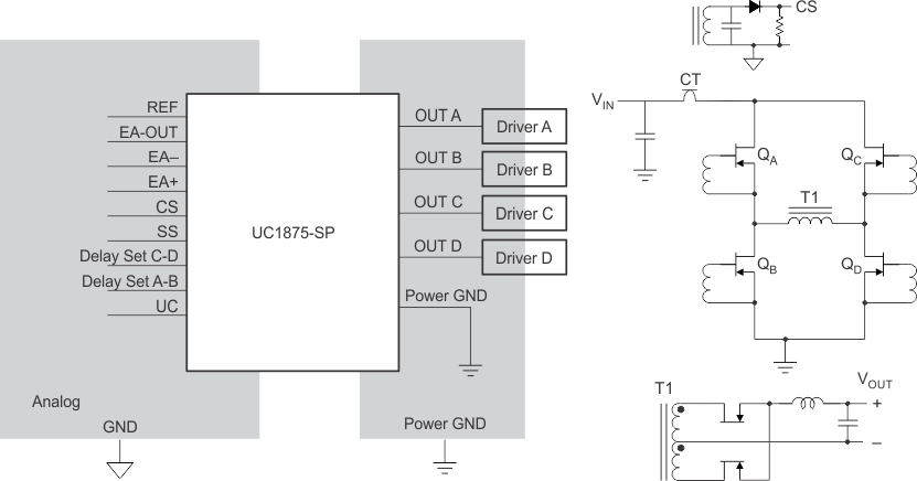
As highlighted in the layout and schematic current is sensed in the input side and not in series with the main transformer. This is to ensue that the current transformer volt-second are balanced i does not flux-walk and saturate. If the current transformer were to be placed in series with the main transformer, if the main transformer were to flux-walk the current transformer will also saturate. Thus having the current transformer in the input side it will ensure to take corrective action to prevent main transformer from saturation.
11.2 Layout Example
 Figure 22. UC1875-SP Based Phase-Shifted Full-Bridge Converter