SLUSAQ9B December 2011 – December 2015 UC1875-SP
PRODUCTION DATA.
- 1 Features
- 2 Applications
- 3 Description
- 4 Revision History
- 5 Description (continued)
- 6 Pin Configuration and Functions
- 7 Specifications
- 8 Detailed Description
-
9 Application and Implementation
- 9.1 Application Information
- 9.2
Typical Application
- 9.2.1 Design Requirements
- 9.2.2
Detailed Design Procedure
- 9.2.2.1 Phase-Shifted Fundamentals
- 9.2.2.2 Circuit Schematic and Description
- 9.2.2.3 Initial Conditions (Time: t = t(0))
- 9.2.2.4 Right Leg Resonant Transition Interval (Time: t(0) < t < t(1))
- 9.2.2.5 Clamped Freewheeling Interval (Time: t(1) < t < t(2))
- 9.2.2.6 Left Leg Transition Interval (Time: t(2) < t < t(3))
- 9.2.2.7 Power Transfer Interval (Time: t(3) < t < t(4))
- 9.2.2.8 Switch Turn Off (Time: t(4))
- 9.2.2.9 Resonant Tank Considerations
- 9.2.2.10 Resonant Circuit Limitations
- 9.2.2.11 Stored Inductive Energy
- 9.2.2.12 Resonant Circuit Summary
- 9.2.2.13 Stored Energy Requirements
- 9.2.2.14 Minimum Primary Current
- 9.2.3 Application Curve
- 10Power Supply Recommendations
- 11Layout
- 12Device and Documentation Support
- 13Mechanical, Packaging, and Orderable Information
パッケージ・オプション
メカニカル・データ(パッケージ|ピン)
サーマルパッド・メカニカル・データ
発注情報
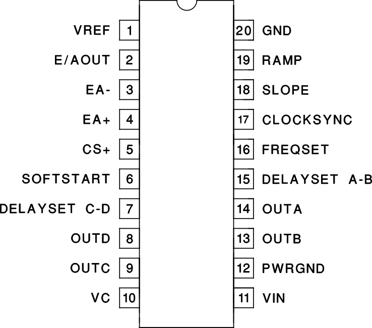
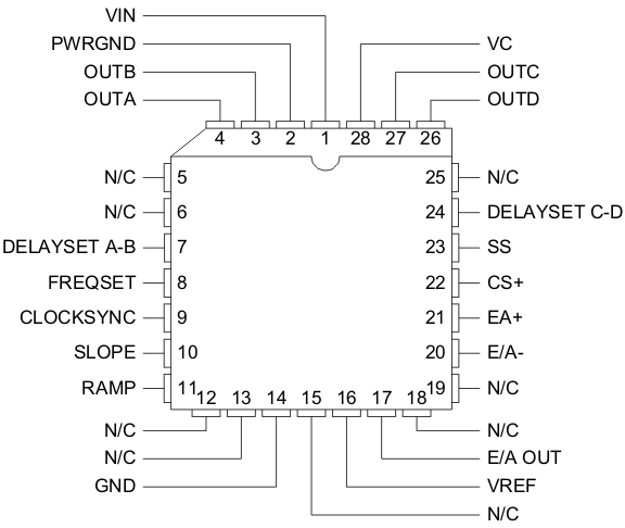
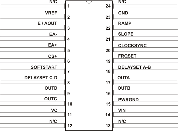
6 Pin Configuration and Functions
J Package
20-Pin CDIP
Top View

FK Package
28-Pin LCCC
Top View

W Package
24-Pin CFP
Top View

Pin Functions
| PIN | I/O | DESCRIPTION | |||
|---|---|---|---|---|---|
| NAME | CDIP | LCCC | CFP | ||
| CLOCK/ SYNC |
17 | 9 | 20 | I/O | Bi-directional clock and synchronization pin. Used as an output, this pin provides a clock signal. As an input, this pin provides a synchronization point. |
| C/S+ | 5 | 22 | 6 | I | The positive input to the current-fault comparator whose reference is set internally to fixed 2.5 V (separate from VREF). When the voltage at this pin exceeds 2.5 V, the current-fault latch is set, the outputs are forced off and a SOFT START cycle is initiated. If a constant voltage above 2.5 V is applied to this pin the outputs are disabled from switching and held in a low state until the C/S (+) pin is brought below 2.5 V. The outputs may begin switching at 0 degrees phase shift before the SOFT START pin begins to rise, this condition will not prematurely deliver power to the load. |
| DELAY SET A/B | 15 | 7 | 18 | O | Output delay control. The users programmed current flowing from these pins to GND set the turn-on delay for the corresponding output pair. This delay is introduced between turn-off of one switch and turn-on of another in the same leg of the bridge to provide a dead time in which the resonant switching of the external power switches takes place. Separate delays are provided for the two half bridges to accommodate differences in the resonant capacitor charging currents. |
| DELAY SET C/D | 7 | 24 | 8 | O | Output delay control. The users programmed current flowing from these pins to GND set the turn-on delay for the corresponding output pair. This delay is introduced between turn-off of one switch and turn-on of another in the same leg of the bridge to provide a dead time in which the resonant switching of the external power switches takes place. Separate delays are provided for the two half bridges to accommodate differences in the resonant capacitor charging currents. |
| E/A+ | 4 | 21 | 5 | I | This pin is normally connected to a reference voltage used for comparison with the sensed power supply output voltage level at the E/A(-) pin. |
| E/A– | 3 | 20 | 4 | I | This pin is normally connected to the voltage divider resistors which sense the power supply output level. |
| E/A OUT (COMP) | 2 | 17 | 3 | O | Error amplifier output. This is the gain stage for overall feedback control. Error amplifier output voltage levels below 1 volt will force 0° phase shift. Since the error amplifier has a relatively low current drive capability, the output may be overridden by driving with a sufficiently low impedance source. |
| FREQ SET | 16 | 8 | 19 | O | Oscillator frequency set pin. A resistor and a capacitor from FREQ SET to GND will set oscillator frequency according to the following relationship: f = 4/(RfSET × CRAMP). |
| GND | 20 | 14 | 23 | _ | Signal ground. All voltages are measured with respect to ground (GND). The timing capacitor, on the FREQ SET pin, and bypass capacitor on the VREF pin, bypass capacitors on VIN and the ramp capacitor, on the RAMP pin, should be connected directly to the ground plane near the signal ground pin. |
| N/C | 5, 6, 12, 13, 15, 18, 19, 25 | 1, 12, 13, 24 | _ | No connection. | |
| OUT A | 14 | 4 | 17 | O | The outputs are 2 A totem-pole drivers optimized for both MOSFET gates and level shifting transformers. The outputs operate as pair with a nominal 50% duty cycle. The A-B pair is intended to drive one half bridge in the external power stage and is synchronized with the clock waveform. The C-D pair will drive the other half-bridge with switching phase shifted with respect to the A-B outputs. |
| OUT B | 13 | 3 | 16 | O | See OUT A description. |
| OUT C | 9 | 27 | 10 | O | See OUT A description. |
| OUT D | 8 | 26 | 9 | O | See OUT A description. |
| POWER GND | 12 | 2 | 15 | _ | Power ground. VC should be bypassed with a ceramic capacitor from the VC pin to the section of the ground plane that is connected to PWR GND. Any required bulk reservoir capacitor should parallel this one. Power ground and signal ground may be joined at a signal point to optimize noise rejection and minimize DC drops. |
| RAMP | 19 | 11 | 22 | I | Voltage ramp. This pin is the input to the pulse width modulator comparator. Connect a capacitor from here to GND. A voltage ramp is developed at this pin with a slope: (dV/dT) = (sense voltage/RSLOPE × CRAMP). |
| SLOPE | 18 | 10 | 21 | I | Set ramp slope compensation. A resistor from this pin to VCC will set the current used to generate the ramp. Connecting this resistor to the DC input line will provide voltage feed forward. |
| SOFT-START | 6 | 23 | 7 | O | SOFT START will remain at GND as long as VIN is below the UVLO threshold. SOFT START will be pulled up to about 4.8 V by an internal 9 μA current source when VIN becomes valid (assuming a non-fault condition). In the event of a current-fault (C/S (+) voltage exceeding 2.5 V), SOFT START will be pulled to GND and then ramp to 4.8 V. If a fault occurs during the SOFT START cycle, the outputs will be immediately disabled and SOFT START must charge fully prior to resetting the fault latch. For paralleled controllers, the SOFT START pins may be paralleled to a single capacitor, but the change currents will be additive. |
| VC | 10 | 28 | 11 | I | Output switch supply voltage. This pin supplies power to the drivers and their associated bias circuitry. Connect VC to a stable source above 3 V for normal operation, above 12 V for best performance. This supply should be bypassed directly to the PWR GND pin with low ESR, low ESL capacitors. |
| VIN | 11 | 1 | 14 | I | Primary chip supply voltage. This pin supplies power to the logic and analog circuitry on the integrated circuitry that is not directly associated with driving the output stages. |
| VREF | 1 | 16 | 2 | I | This pin is an accurate 5 V voltage reference. This output is capable of delivering about 60 mA to peripheral circuitry and is internally short circuit current limited. |
Table 1. Under Voltage Threshold (UVLO)
| UVLO TURN-ON | UVLO TURN-OFF | DELAY SET | |
|---|---|---|---|
| UCC1875-SP | 10.75V | 9.25V | Yes |