SLUSAQ9B December 2011 – December 2015 UC1875-SP
PRODUCTION DATA.
- 1 Features
- 2 Applications
- 3 Description
- 4 Revision History
- 5 Description (continued)
- 6 Pin Configuration and Functions
- 7 Specifications
- 8 Detailed Description
-
9 Application and Implementation
- 9.1 Application Information
- 9.2
Typical Application
- 9.2.1 Design Requirements
- 9.2.2
Detailed Design Procedure
- 9.2.2.1 Phase-Shifted Fundamentals
- 9.2.2.2 Circuit Schematic and Description
- 9.2.2.3 Initial Conditions (Time: t = t(0))
- 9.2.2.4 Right Leg Resonant Transition Interval (Time: t(0) < t < t(1))
- 9.2.2.5 Clamped Freewheeling Interval (Time: t(1) < t < t(2))
- 9.2.2.6 Left Leg Transition Interval (Time: t(2) < t < t(3))
- 9.2.2.7 Power Transfer Interval (Time: t(3) < t < t(4))
- 9.2.2.8 Switch Turn Off (Time: t(4))
- 9.2.2.9 Resonant Tank Considerations
- 9.2.2.10 Resonant Circuit Limitations
- 9.2.2.11 Stored Inductive Energy
- 9.2.2.12 Resonant Circuit Summary
- 9.2.2.13 Stored Energy Requirements
- 9.2.2.14 Minimum Primary Current
- 9.2.3 Application Curve
- 10Power Supply Recommendations
- 11Layout
- 12Device and Documentation Support
- 13Mechanical, Packaging, and Orderable Information
パッケージ・オプション
メカニカル・データ(パッケージ|ピン)
サーマルパッド・メカニカル・データ
発注情報
7 Specifications
7.1 Absolute Maximum Ratings
over operating free-air temperature range (unless otherwise noted)(1)(2)| MIN | MAX | UNIT | ||
|---|---|---|---|---|
| Supply voltage (VC, VIN) | 20 | V | ||
| Output current, source or sink | DC | 0.5 | A | |
| Pulse (0.5 µs) | 3 | A | ||
| Analog inputs | (Pins 1, 2, 3, 4, 5, 6, 7, 15, 16, 17, 18, 19) | –0.3 | 5.3 | V |
| Maximum junction temperature, JTmax | 150 | |||
| Thermal Resistance, RθJC(top) | J package | 7 | °C/W | |
| W package | 5.4 | |||
| FK package | 5.6 | |||
| Storage temperature, Tstg | –65 | 150 | °C | |
(1) Stresses beyond those listed under Absolute Maximum Ratings may cause permanent damage to the device. These are stress ratings only, which do not imply functional operation of the device at these or any other conditions beyond those indicated under Recommended Operating Conditions. Exposure to absolute-maximum-rated conditions for extended periods may affect device reliability.
(2) Pin references are to 20-pin packages. All voltages are with respect to ground. Currents are positive into, negative out of the device terminals.
7.2 ESD Ratings
| VALUE | UNIT | |||
|---|---|---|---|---|
| V(ESD) | Electrostatic discharge | Human-body model (HBM), per ANSI/ESDA/JEDEC JS-001(1) | ±1000 | V |
(1) JEDEC document JEP155 states that 500-V HBM allows safe manufacturing with a standard ESD control process.
7.3 Recommended Operating Conditions
over operating free-air temperature range (unless otherwise noted)| MIN | NOM | MAX | UNIT | ||
|---|---|---|---|---|---|
| Supply Voltage Vin | 10.75 | 12 | 18 | V | |
7.4 Thermal Information
| THERMAL METRIC(1) | UC1875-SP | UNIT | |||
|---|---|---|---|---|---|
| J (CDIP) | FK (LCCC) | W (CFP) | |||
| 20 PINS | 28 PINS | 24 PINS | |||
| RθJC(top) | Junction-to-case (top) thermal resistance | 6.2 | 8.2 | 4.8 | °C/W |
(1) For more information about traditional and new thermal metrics, see the Semiconductor and IC Package Thermal Metrics application report, SPRA953.
7.5 Electrical Characteristics
–55°C < TA < 125°C. VC = VIN = 12 V, R(FREQSET) = 12 kΩ, C(FREQSET) = 330 pF, R(SLOPE) = 12 kΩ, C(RAMP) = 200 pF,C(DELAYSET A-B) = C(DELAYSET C-D) = 0.01 µF, I(DELAYSET A-B) = I(DELAYSET C-D) = –500 µA, TA = TJ, unless otherwises stated.
| PARAMETER | TEST CONDITIONS | MIN | TYP | MAX | UNIT | ||
|---|---|---|---|---|---|---|---|
| UNDERVOLTAGE LOCKOUT | |||||||
| Start threshold | 10.75 | 11.75 | V | ||||
| UVLO hysteresis | 0.5 | 1.25 | 2 | V | |||
| SUPPLY CURRENT | |||||||
| IIN Startup | VIN = 8 V, VC = 20 V, R(SLOPE) open, I(DELAY) = 0 |
150 | 600 | μA | |||
| IC Startup | VIN = 8 V, VC = 20 V, R(SLOPE) open, I(DELAY) = 0 |
10 | 100 | µA | |||
| IIN | 30 | 44 | mA | ||||
| IC | 15 | 30 | mA | ||||
| VOLTAGE REFERENCE | |||||||
| Output voltage | TJ = 25°C | 4.92 | 5 | 5.08 | V | ||
| Line regulation | 11 V < VIN < 20 V | 1 | 10 | mV | |||
| Load regulation | IVREF = –10 mA | 5 | 20 | mV | |||
| Total variation | Line, Load, Temperature | 4.9 | 5.1 | V | |||
| Noise Voltage | 10 Hz to 10 kHz | 50 | µVrms | ||||
| Long Term Stability | TJ = 125°C, 1000 hours | 2.5 | mV | ||||
| Short circuit current | VREF = 0 V, TJ = 25°C | 60 | mA | ||||
| ERROR AMPLIFIER | |||||||
| Offset voltage | 5 | 15 | mV | ||||
| Input bias current | 0.6 | 3 | μA | ||||
| AVOL | 1 V < V(E/AOUT) < 4 V | 60 | 90 | dB | |||
| CMMR | 1.5 V < VCM < 5.5 V | 75 | 95 | dB | |||
| PSRR | 11 V < VIN < 20 V | 85 | 100 | dB | |||
| Output sink current | V(E/AOUT) = 1 V | 1 | 2.5 | mA | |||
| Output source current | I(E/AOUT) = 4 V | –1.3 | –0.5 | mA | |||
| Output voltage high | I (E/AOUT) = –0.5 mA | 4 | 4.7 | 5 | V | ||
| Output voltage low | I(E/AOUT) = 1 mA | 0 | 0.5 | 1 | V | ||
| Unity Gain BW | See (7) | 01 device | 5 | MHz | |||
| 02 device | 7 | ||||||
| Slew rate | See (7) | 6 | 11 | V/μs | |||
| PWM COMPARATOR | |||||||
| RAMP offset voltage | TJ = 25°C(2) | 1.3 | V | ||||
| Zero phase shift voltage | See (3) | 0.55 | 0.9 | V | |||
| PWM phase shift (1)(6) | V(E/AOUT) > (Ramp Peak + Ramp Offset) | 01 device | 98% | 99.5% | 102% | ||
| 02 device | 96% | 100% | 104% | ||||
| V(E/AOUT) < Zero Phase Shift Voltage | 0% | 0.5% | 2% | ||||
| Output skew (1) (6) | V(E/AOUT) > 1 V | 5 | ±20 | ns | |||
| Ramp to output delay (5) (7) | 65 | 125 | |||||
| OSCILLATOR | |||||||
| Initial accuracy | TA = 25°C | 01 device | 0.85 | 1 | 1.15 | MHz | |
| 02 device | 0.85 | 1 | 1.19 | ||||
| Voltage stability | 11 V < VIN < 20 V | 0.2% | 2% | ||||
| Total variation | Line, Temperature | 0.8 | 1.2 | MHz | |||
| Sync pin threshold | TJ = 25°C | 3.8 | V | ||||
| Clock out peak | TJ = 25°C | 4.3 | V | ||||
| Clock out low | TJ = 25°C | 3.3 | V | ||||
| Clock out pulse width | R(CLOCKSYNC) = 3.9 kΩ | 30 | 100 | ns | |||
| Maximum frequency (6) | R(FREQUEST) = 5 kΩ | 2 | MHz | ||||
| RAMP GENERATOR/SLOPE COMPENSATION | |||||||
| Ramp current, minimum | I(SLOPE) = 10 µA, V(FREQSET) = VREF | –11 | –14 | µA | |||
| Ramp current, maximum | I(SLOPE) = 1 mA, V(FREQSET) = VREF | –0.8 | –0.95 | mA | |||
| Ramp valley | 0 | V | |||||
| Ramp peak - clamping level | R(FREQSET) = 100 kΩ | 3.8 | 4.1 | 5 | V | ||
| CURRENT LIMIT | |||||||
| Input bias | VCS+ = 3 V | 2 | 5 | μA | |||
| Threshold voltage | 2.4 | 2.5 | 2.6 | V | |||
| Delay to output (7) | 85 | 150 | ns | ||||
| SOFT START/RESET DELAY | |||||||
| Charge current | V(SOFTSTART) = 0.5 V | –20 | –9 | –3 | μA | ||
| Discharge current | V(SOFTSTART) = 1 V | 120 | 230 | µA | |||
| Restart threshold | 4.3 | 4.7 | V | ||||
| Discharge level | 300 | mV | |||||
| OUTPUT DRIVERS | |||||||
| Output low level | IOUT = 50 mA | 0.2 | 0.4 | V | |||
| Output high level | IOUT = –50 mA | 1.5 | 2.5 | V | |||
| DELAY SET | |||||||
| Delay set voltage | I(DELAY) = –500 µA | 2.3 | 2.4 | 2.6 | V | ||
| Delay time (7) | I(DELAY) = –250 µA (4) | 150 | 250 | 600 | ns | ||
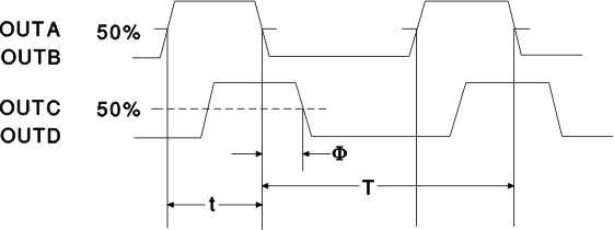
(1) Phase shift percentage (0% = 0 , 100% = 180 ) is defined as  where is the phase shift, and and T are defined in Figure 1. At 0% phase shift, is the output skew.
 where is the phase shift, and and T are defined in Figure 1. At 0% phase shift, is the output skew.
(2) Ramp offset voltage has a temperature coefficient of about –4 mV/°C.
(3) The zero phase shift voltage has a temperature coefficient of about –2 mV/°C.
(4) Delay time can be programmed via resistors from the delay set pins to ground. Delay time =  .
.
Where I(DELAY) = . The Recommended range for I(DELAY) is 25 µA ≤ I(DELAY) ≤ 1 mA.
 .
.Where I(DELAY) =
 . The Recommended range for I(DELAY) is 25 µA ≤ I(DELAY) ≤ 1 mA.
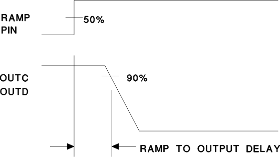
(5) Ramp delay to output time is defined in Figure 1
(6) Not production tested at –55·C.
(7) Not production tested.

Duty Cycle = t/T, Period = T
TDHL (A to C) = TDHL (B to D) = Φ
Figure 1. Phase Shift, Output Skew and Delay Time Definitions
 Figure 2. Ramp to Delay Output